MT8941B 데이터 시트보기 (PDF) - Zarlink Semiconductor Inc
부품명
상세내역
일치하는 목록
MT8941B Datasheet PDF : 27 Pages
| |||
MT8941B
Data Sheet
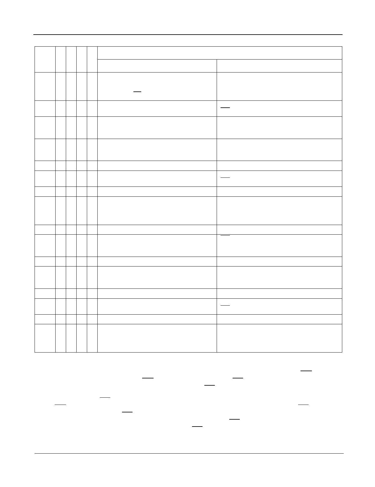
Mode
#
MMMM
SSSS
0123
DPLL #1
Operating Modes
DPLL #2
NORMAL MODE:
Properly phase related External 4.096 MHz
Provides the T1 (1.544 MHz) clock
clock and 8 kHz frame pulse provide the ST-
0 0 0 0 0 synchronized to the falling edge of the input BUS clock at 2.048 MHz.
frame pulse (F0i).
1 0 0 0 1 NORMAL MODE
NORMAL MODE:
F0b is an input but has no function in this mode.
2 0 0 1 0 NORMAL MODE
External 4.096 MHz provides the ST-BUS clock
and Frame Pulse at 2.048 MHz and 8 kHz,
respectively.
NORMAL MODE
3 0011
NORMAL MODE:
Provides the CEPT/ST-BUS compatible timing
signals locked to the 8 kHz input signal (C8Kb).
4 0 1 0 0 DIVIDE-1 MODE
Same as mode ‘0’.
5 0 1 0 1 DIVIDE-1 MODE
SINGLE CLOCK-1 MODE
F0b is an input but has no function in this mode.
6 0 1 1 0 DIVIDE-1 MODE
Same as mode 2.
DIVIDE-1 MODE:
Divides the CVb input by 193. The divided
7 0 1 1 1 output is connected to DPLL #2.
SINGLE CLOCK-1 MODE:
Provides the CEPT/ST-BUS compatible timing
signals locked to the 8 kHz internal signal
provided by DPLL #1.
8 1 0 0 0 NORMAL MODE
Same as mode ‘0’.
NORMAL MODE
9 1001
F0b is an input and DPLL #2 locks on to
it only if it is at 16 kHz to provide the ST-BUS
control signals.
10 1 0 1 0 NORMAL MODE
Same as mode 2.
NORMAL MODE
11 1 0 1 1
FREE-RUN MODE:
Provides the ST-BUS timing signals with no
external inputs except the master clock.
12 1 1 0 0 DIVIDE-2 MODE
Same as mode ‘0’.
13 1 1 0 1 DIVIDE-2 MODE
SINGLE CLOCK-2 MODE:
F0b is an input but has no function in this mode.
14 1 1 1 0 DIVIDE-2 MODE
Same as mode 2.
DIVIDE-2 MODE:
Divides the CVb input by 256. The divided
15 1 1 1 1 output is connected to DPLL#2.
SINGLE CLOCK-2 MODE:
Provides the CEPT/ST-BUS compatible timing
signals locked to the 8 kHz internal signal
provided by DPLL #1.
Table 4 - Summary of Modes of Operation - DPLL #1 and #2
When MS3 is HIGH, DPLL #2 operates in any of the major modes selected by MS0 and MS1. When MS3 is LOW,
it overrides the major mode selected and DPLL#2 accepts an external clock of 4.096 MHz on C4b (pin 13) to
provide the 2.048 MHz clocks (C2o and C2o) and the 8 kHz frame pulse (F0b) compatible with the ST-BUS format.
The mode select bit MS2 controls the direction of the signal on F0b (pin 6).
When MS2 is LOW, the F0b pin is an 8 kHz frame pulse input. This input is effective only when MS3 is also LOW
and pin C4b is fed by a 4.096 MHz clock, which has a proper phase relationship with the signal on F0b (refer Figure
18). Otherwise, the input on pin F0b will have no bearing on the operation of DPLL #2, unless it is in FREE-RUN
mode as selected by MS0 and MS1. In FREE-RUN mode, the input on F0b is treated the same way as the C8Kb
input is in NORMAL mode. The frequency of the signal on F0b should be 16 kHz for DPLL #2 to lock and generate
the ST-BUS compatible clocks at 4.096 MHz and 2.048 MHz.
8
Zarlink Semiconductor Inc.
Share Link: 