MT8941B 데이터 시트보기 (PDF) - Zarlink Semiconductor Inc
부품명
상세내역
일치하는 목록
MT8941B Datasheet PDF : 27 Pages
| |||
MT8941B
Data Sheet
M
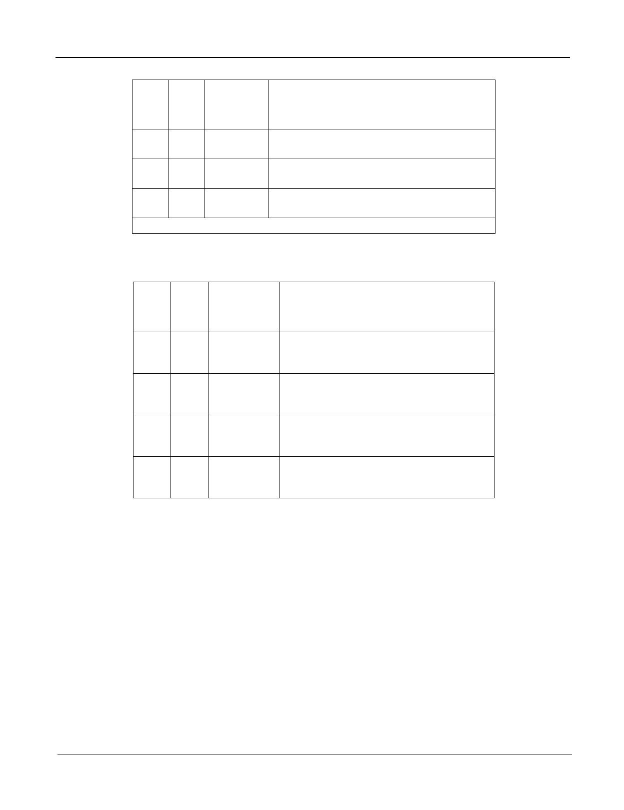
M
Mode of
S
S
Operation
0
1
Function
X
0 NORMAL Provides the T1 (1.544 MHz) clock synchronized
to the falling edge of the input frame pulse (F0i).
0
1 DIVIDE-1 DPLL #1 divides the CVb input by 193. The
divided output is connected to DPLL #2.
1
1 DIVIDE-2 DPLL #1 divides the CVb input by 256. The
divided output is connected to DPLL #2.
Note: X: indicates don’t care
Table 1 - Major Modes of DPLL #1
M
M
Mode of
S
S
Operation
0
1
Function
0
0
NORMAL Provides CEPT/ST-BUS timing signals locked
to the falling edge of the 8 kHz input signal at
C8Kb.
1
0 FREE-RUN Provides CEPT/ST-BUS timing and framing
signals with no external inputs, except the
master clock.
0
1
SINGLE Provides CEPT/ST-BUS timing signals locked
CLOCK-1 to the falling edge of the 8 kHz internal signal
provided by DPLL #1.
1
1
SINGLE Provides CEPT/ST-BUS timing signals locked
CLOCK-2 to the falling edge of the 8 kHz internal signal
provided by DPLL #1.
Table 2 - Major Modes of DPLL #2
6
Zarlink Semiconductor Inc.
Share Link: 