MT8941B 데이터 시트보기 (PDF) - Zarlink Semiconductor Inc
부품명
상세내역
일치하는 목록
MT8941B Datasheet PDF : 27 Pages
| |||
MT8941B
Data Sheet
Functional Description
The MT8941B is a dual digital phase-locked loop providing the timing and synchronization signals to the interface
circuits for T1 and CEPT (30+2) Primary Multiplex Digital Transmission links. As shown in the functional block
diagram (see Figure 1), the MT8941B has two digital phase-locked loops (DPLLs), associated output controls and
the mode selection logic circuits. The two DPLLs, although similar in principle, operate independently to provide T1
(1.544 MHz) and CEPT (2.048 MHz) transmission clocks and ST-BUS timing signals.
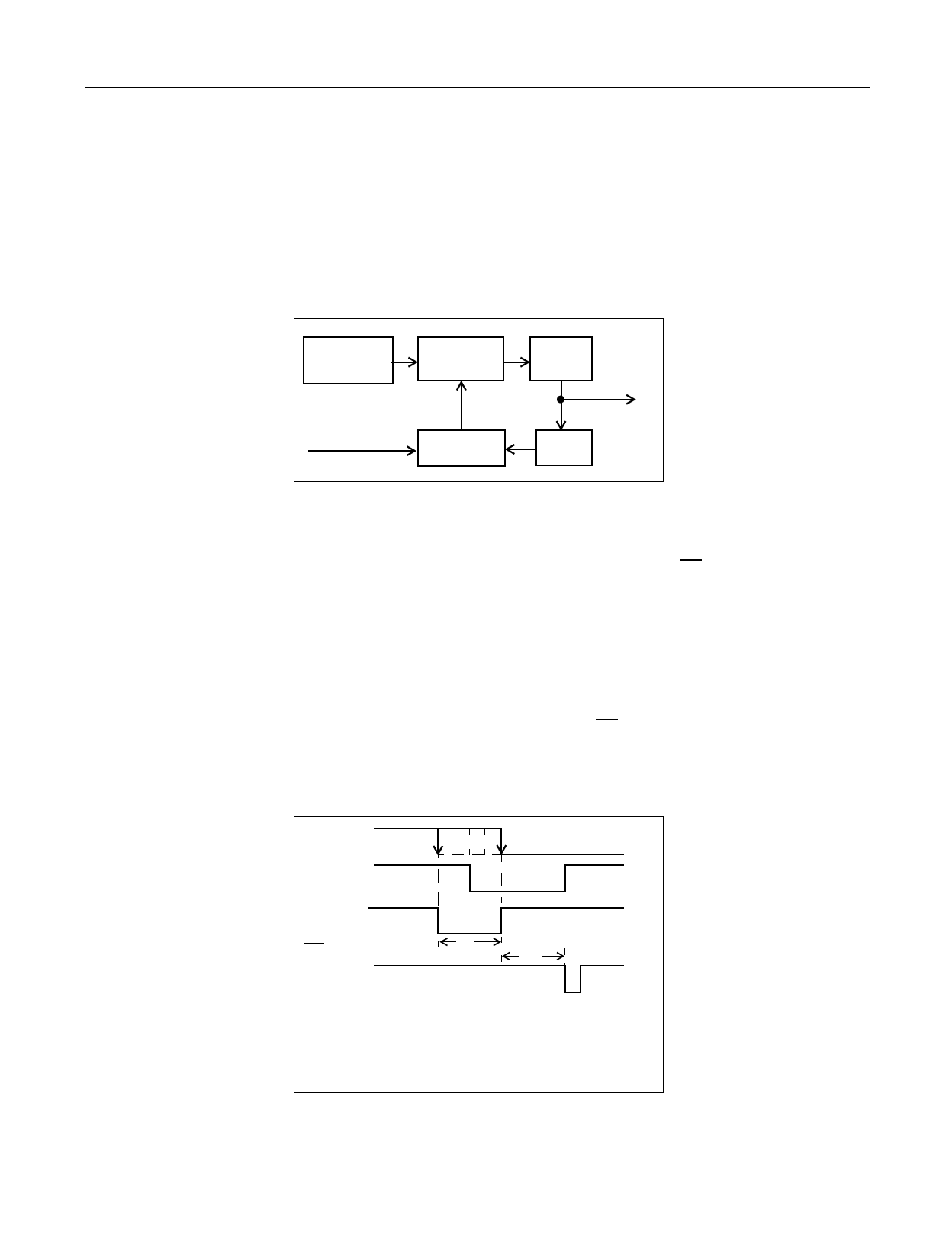
The principle of operation behind the two DPLLs is shown in Figure 3. A master clock is divided down to 8 kHz
where it is compared with the 8 kHz input, and depending on the output of the phase comparison, the master clock
frequency is corrected.
Master clock
(12.352 MHz /
16.384 MHz)
Frequency
Correction
Input (8 kHz)
Phase
Comparison
÷8
Output
(1.544 MHz /
2.048 MHz)
÷ 193 /
÷ 256
Figure 3 - DPLL Principle
The MT8941B achieves the frequency correction in both directions by using three methods; speed-up, slow-down
and no-correction.
As shown in Figure 4, the falling edge of the 8 kHz input signal (C8Kb for DPLL #2 or F0i for DPLL # 1) is used to
sample the internally generated 8 kHz clock and the correction signal (CS) once in every frame (125 µs). If the
sampled CS is “1”, then the DPLL makes a speed-up or slow-down correction depending upon the sampled value
of the internal 8 kHz signal. A sampled ”0” or “1” causes the frequency correction circuit to respectively stretch or
shrink the master clock by half a period at one instant in the frame. If the sampled CS is “0”, then the DPLL makes
no correction on the master clock input. Note that since the internal 8 kHz signal and the CS signal are derived from
the master clock, a correction will cause both clocks to stretch or shrink simultaneously by an amount equal to half
the period of the master clock.
Once in synchronization, the falling edge of the reference signal (C8Kb or F0i) will be aligned with either the falling
or the rising edge of CS. It is aligned with the rising edge of CS when the reference signal is slower than the internal
8 kHz signal. On the other hand, the falling edge of the reference signal will be aligned with the falling edge of CS
if the reference signal is faster than the internal 8 kHz signal.
C8Kb (DPLL #2)
or F0i (DPLL #1)
Internal
8 kHz
correction
CS
speed-up
region
F0b
(DPLL #2)
tCS
no-correction
sampling edge
correction
slow-down
region
tCSF
DPLL #1: tCS = 4 × TP12 ± 0.5 × TP12
DPLL #2: tCS = 512 × TP16 ± 0.5 × TP16
tCSF = 766 × TP16
where, TP12 is the 12.352 MHz master clock oscillator period
for DPLL #1 and TP16 is the 16.384 MHz master clock period
for DPLL #2.
Figure 4 - Phase Comparison
4
Zarlink Semiconductor Inc.
Share Link: 