MT8941B 데이터 시트보기 (PDF) - Zarlink Semiconductor Inc
부품명
상세내역
일치하는 목록
MT8941B Datasheet PDF : 27 Pages
| |||
MT8941B
Data Sheet
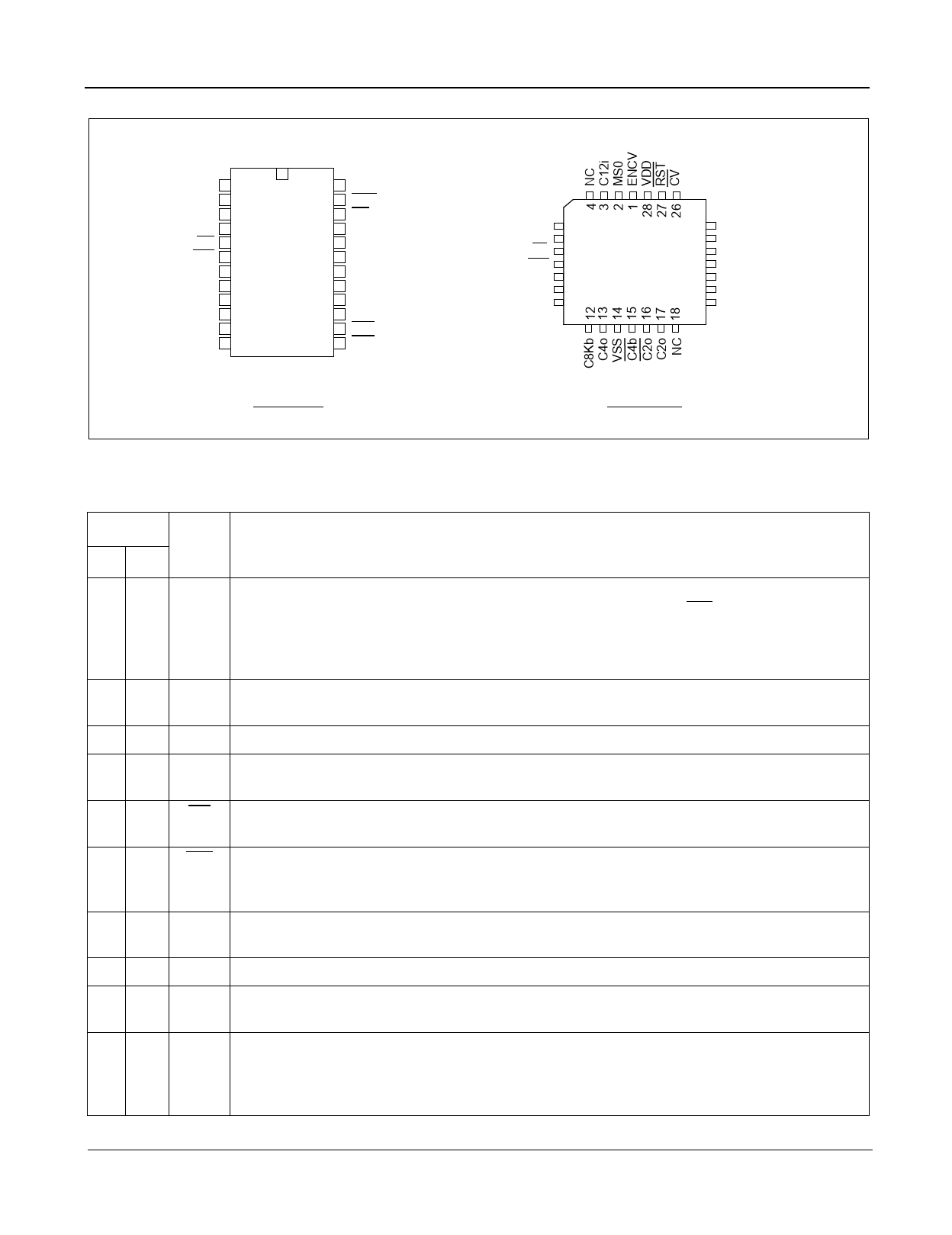
ENVC 1
MS0 2
C12i 3
MS1 4
F0i 5
F0b 6
MS2 7
C16i 8
ENC4o 9
C8Kb 10
C4o 11
VSS 12
24 VDD
23 RST
22 CV
21 CVb
20 Yo
19 Bi
18 Ai
17 MS3
16 ENC2o
15 C2o
14 C2o
13 C4b
NC 5
•
25 NC
MS1 6
24 CVb
F0i 7
23 Yo
F0b 8
22 Bi
MS2 9
21 Ai
C16i 10
20 MS3
ENC4o 11
19 ENC2o
24 PIN PDIP
28 PIN PLCC
Figure 2 - Pin Connections
Pin Description
Pin #
Name
DIP PLCC
Description
1 1 ENCV Variable clock enable (TTL compatible input) - This input directly controls the three states
of CV (pin 22) under all modes of operation. When HIGH, enables CV and when LOW, puts
it in high impedance condition. It also controls the three states of CVb signal (pin 21) if MS1
is LOW. When ENCV is HIGH, the pin CVb is an output and when LOW, it is in high
impedance state. However, if MS1 is HIGH, CVb is always an input.
2 2 MS0 Mode select ‘0’ input (TTL compatible) - This input in conjunction with MS1 (pin 4) selects
the major mode of operation for both DPLLs. (Refer to Tables 1 and 2.)
3 3 C12i 12.352 MHz Clock input (TTL compatible) - Master clock input for DPLL #1.
4 6 MS1 Mode select-1 input (TTL compatible) - This input in conjunction with MS0 (pin 2) selects
the major mode of operation for both DPLLs. (Refer to Tables 1 and 2.)
57
F0i Frame pulse input (TTL compatible) - This is the frame pulse input at 8 kHz. DPLL #1
locks to the falling edge of this input to generate T1 (1.544 MHz) clock.
68
F0b Frame pulse Bidirectional (TTL compatible input and Totem-pole output) - Depending
on the minor mode selected for DPLL #2, it provides the 8 kHz frame pulse output or acts as
an input to an external frame pulse.
7 9 MS2 Mode select-2 input (TTL compatible) - This input in conjunction with MS3 (pin 17) selects
the minor mode of operation for DPLL #2. (Refer to Table 3.)
8 10 C16i 16.384 MHz Clock input (TTL compatible) - Master clock input for DPLL #2.
9 11 ENC4o Enable 4.096 MHz clock (TTL compatible input) - This active high input enables C4o (pin
11) output. When LOW, the output C4o is in high impedance condition.
10 12 C8Kb Clock 8 kHz Bidirectional (TTL compatible input and Totem-pole output) - This is the 8
kHz input signal on the falling edge of which the DPLL #2 locks during its NORMAL mode.
When DPLL #2 is in SINGLE CLOCK mode, this pin outputs an 8 kHz internal signal
provided by DPLL #1 which is also connected internally to DPLL #2.
2
Zarlink Semiconductor Inc.
Share Link: 