73M2910L 데이터 시트보기 (PDF) - TDK Corporation
부품명
상세내역
일치하는 목록
73M2910L Datasheet PDF : 35 Pages
| |||
73M2910L
Microcontroller
BIT 4 Clock 2 Output Enable
Bit 4 enables the clock at the CLOCK 2 output pin if it is set to a 1. The CLOCK 2 pin output is held to a 0, by
writing this bit to a 0. This will reduce system power if the clock pin is not used or if a power reduction mode is
required.
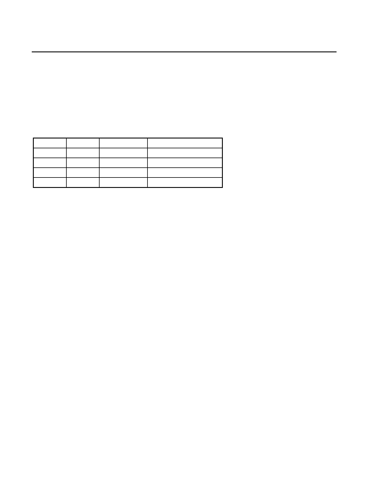
BITS 3,2 Clock 2 Output Control
These bits determine the oscillator divisor for the CLOCK 2 output pin. They were designed to provide a
1.8432 MHz clock for an external UART given an oscillator frequency of 11.0592 MHz, 22.1184 MHz,
18.432 MHz, or 13.824 MHz.
BIT 3
0
0
1
1
BIT 2
0
1
0
1
CLK 2 OUT
OSC/7.5
OSC/6
OSC/12
OSC/10
OSC FREQUENCY
13.824 MHz
11.059 MHz
22.118 MHz
18.432 MHz
BIT 1 Clock 1 Output Enable
Bit 1 enables the clock at the clock 1 output pin if it is set to a 1. The clock pin output is held to a 0, by writing a
0 to this bit. This will reduce system power if the clock pin is not used or if a power reduction mode is required.
Bit 6 is cleared to a 0 upon a reset.
BIT 0 Clock 1 Output Control
Bit 0 controls the frequency of the clock 1 output pin. The clock output is either the oscillator’s output signal
divided by two or a buffered oscillator output signal.
POWER SAVING MODES
Low Power Modes
The 73M2910L supports two power conservation modes, which are controlled by the PCON.1 and PCON.0
control bits of the PCON Register.
If PCON.0 is set, the 73M2910L will go into a power saving mode where the oscillator is running, clocks are
supplied to the UART, timers, HDLC, and interrupt blocks, but no clocks are supplied to the CPU. Instruction
processing and activity on the address and data ports is halted. Normal operation is resumed when an
unmasked interrupt is requested or when a reset occurs.
If PCON.1 is set, the 73M2910L goes into its lowest power mode where the oscillator is halted. The total current
consumption in this state should be less than 10 µa. The 73M2910L will start its oscillator and begin to return to
normal operation when either a reset occurs, when a falling (rising if corresponding direction bit is set) edge of
an unmasked external interrupt from pins INT(2:0) is detected, or when the USR5 (1:0) pins change to a state
according to the USR5 port register. Edges used in wakeup modes are not filtered in the
73M2910L, so the user must be cautious of noise or small glitches inadvertently waking up the chip. From the
time the edge that results in the wake up occurs, to the point at which an instruction is executed, depends on
the oscillator start-up time. Three good oscillator pulses must be detected before the main internal clocks are
generated.
During power-down mode, both the ALE and PSEN pins are pulled high since these signals often provide the
output enable and chip enable for the ROM (active low). This ensures that the external components are in their
lowest power state.
5
Share Link: 