73M2910L 데이터 시트보기 (PDF) - TDK Corporation
부품명
상세내역
일치하는 목록
73M2910L Datasheet PDF : 35 Pages
| |||
73M2910L
Microcontroller
USR PROGRAMMABLE I/O (continued)
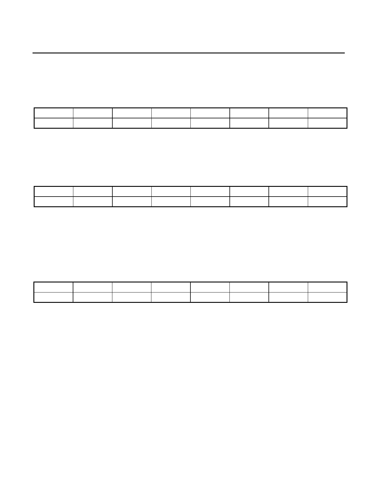
USR4 PORT
USR4 Port Data External Address 0003h
Byte Addressable
Reset State 00h
BIT 7
USR4.7
BIT 6
USR4.6
BIT 5
USR4.5
BIT 4
USR4.4
BIT 3
USR4.3
BIT 2
USR4.2
BIT 1
USR4.1
BIT 0
USR4.0
Bits in this register will be asserted on the USR4(7:0) pins if the corresponding direction register bit is a 0 and if
the corresponding bit in the Chip Select Enable Register, 0005, is set to a 0. Reading this register will return
data reflecting the values of pins USR4(7:0).
USR4 I/O Port Direction (DIR4) External Address 0004h
Byte Addressable
Reset State FFh
BIT 7
DIR4.7
BIT 6
DIR4.6
BIT 5
DIR4.5
BIT 4
DIR4.4
BIT 3
DIR4.3
BIT 2
DIR4.2
BIT 1
DIR4.1
BIT 0
DIR4.0
This register is used to designate the USR4 pins as either inputs or outputs. If the register bit is reset to a 0, the
corresponding USR4 pin is programmed as an output that will be driven by the corresponding USR4 I/O data
register bit if the corresponding bit in the Chip Select Enable Register, 0005, is set to a 0. If the register bit is a
1, the corresponding pin will treated as an input only if the corresponding bit in register 0005 is set to a 0.
After a reset, the USR4 pins will act as chip select outputs.
USR4 Port Chip Select Enable (CSEN) External Address 0005h
Byte Addressable
Reset State FFh
BIT 7
CSEN 7
BIT 6
CSEN 6
BIT 5
CSEN 5
BIT 4
CSEN 4
BIT 3
CSEN 3
BIT 2
CSEN 2
BIT 1
CSEN 1
BIT 0
CSEN 0
This register is used to designate the USR4 pins as either user programmable I/Os or as chip select
(CS0B - CS7B) functions on a pin by pin basis. This feature is designed to help reduce external glue logic for
peripheral memory mapped devices. The chip select function is programmed by setting the appropriate bits in
the CSEN Register. When a chip select pin is enabled by setting the corresponding CSEN bit to a 1, all data
and direction information from registers 0003 and 0004 for this bit are ignored and the selected port becomes
an output. If the bit is reset to a 0, the pin will be treated as a normal programmable user I/O pin as defined by
registers 0003 and 0004.
The chip select pins have a defined memory map. The intent is that the outputs can be wire OR’ed together for
a flexible selection of peripheral chip selects. All chip selects will be disabled (forced to a logic 1. It is assumed
that all chip selects are active low) after the read or write is completed, and the appropriate chip select will be
enabled as the next new external addresses is asserted. After a reset, the CSB pull-up devices are all enabled,
that is, all chip select outputs are high. Users must account for this if these pins are intended to be general
purpose I/Os.
10
Share Link: 