MT8940 데이터 시트보기 (PDF) - Mitel Networks
부품명
상세내역
일치하는 목록
MT8940 Datasheet PDF : 16 Pages
| |||
ISO-CMOS MT8940
signals are the 4.096 MHz (C4o and C4b) and the
2.048 MHz (C2o and C2o) clocks, and the 8 kHz
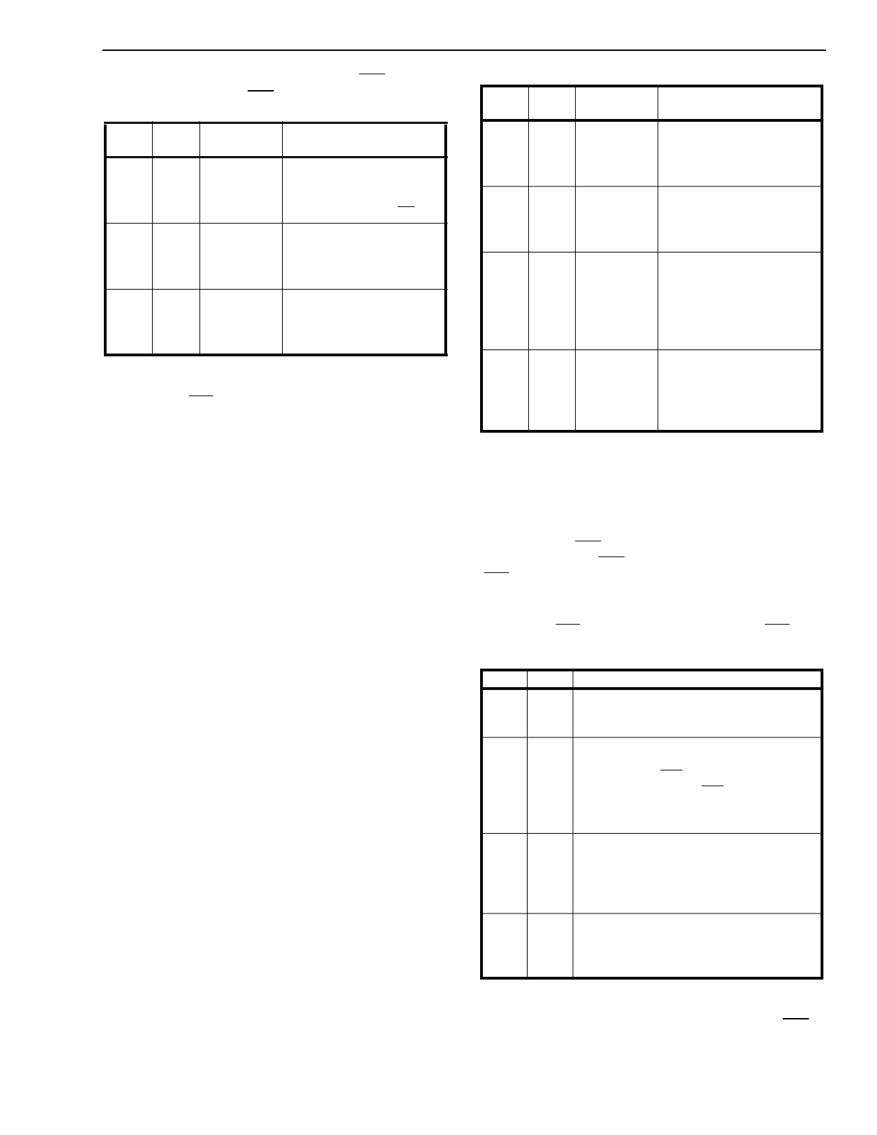
MS0
MS1
Mode of
operation
Function
X
0
NORMAL Provides the T1 (1.544
MHz) clock synchronized
to the falling edge of the
input frame pulse (F0i).
0
1
DIVIDE-1 DPLL #1 divides the CVb
input by 193. The divided
output is connected to
DPLL #2.
1
1
DIVIDE-2 DPLL #1 divides the CVb
input by 256. The divided
output is connected to
DPLL #2.
Note: X: indicates don’t care
Table 1. Major Modes of the DPLL #1
frame pulse (F0b), which are derived from the 16.388
MHz master clock. This mode can also provide the
ST-BUS timing and framing signals with the input
(C8Kb) tied HIGH and the master clock set at 16.384
MHz. The DPLL makes no correction in this
configuration and provides the timing signals
compatible to the ST-BUS format without any jitter.
In FREE-RUN mode, DPLL #2 generates CEPT and
ST-BUS timing and framing signals with no external
inputs except the master clock set at 16.388 MHz.
Since the master clock source is set at a higher
frequency than the nominal value, the DPLL makes
the necessary corrections to deliver the averaged
timing signals compatible to the ST-BUS format.
The operation of DPLL #2 in SINGLE CLOCK-1
mode is identical to SINGLE CLOCK-2 mode,
providing the CEPT and ST-BUS compatible timing
signals synchronized to the internal 8 kHz signal
obtained from DPLL#1 in DIVIDE mode. When
SINGLE CLOCK-1 mode is selected for DPLL #2, it
automatically selects the DIVIDE-1 mode for DPLL
#1, and thus, an external 1.544 MHz clock signal
applied at CVb (pin 21) is divided by DPLL #1 to
generate the internal signal at 8 kHz onto which
DPLL #2 locks. Similarly when SINGLE CLOCK-2
mode is selected, DPLL #1 is in DIVIDE-2 mode,
with an external signal of 2.048 MHz providing the
internal 8 kHz signal to DPLL #2. In both these
modes, this internal signal is available on C8Kb (pin
10) and DPLL #2 locks to its falling edge to provide
the CEPT and ST-BUS compatible timing signals.
This is in contrast to the Normal mode where these
timing signals are synchronized with the rising edge
of the 8 kHz signal on C8Kb.
Minor modes of the DPLL #2
The minor modes for DPLL #2 depends upon the
status of the mode select bits MS2 and MS3 (pins 7
and 17).
MS0
0
1
0
1
MS1
0
0
1
1
Mode of
operation
Function
NORMAL Provides ST-BUS/CEPT
timing signals locked to the
rising edge of the 8kHz
input signal at C8Kb.
FREE-RUN Provides ST-BUS timing
and framing signals with no
external inputs, except the
master clock.
SINGLE Provides the CEPT/ST-
CLOCK-1 BUS compatible timing
signals locked to the falling
edge of the 8kHz internal
signal provided by DPLL
#1.
SINGLE Provides CEPT/ST-BUS
CLOCK-2 timing signals locked to the
falling edge of the 8kHz
internal signal provided by
DPLL #1.
Table 2. Major Modes of the DPLL #2
When MS3 is HIGH, DPLL #2 operates in any of the
major modes as selected by MS0 and MS1.
When MS3 is LOW, it overrides the major mode
selected and DPLL #2 accepts an external clock of
4.096 MHz on C4b (pin 13) to provide the 2.048 MHz
clocks (C2o and C2o) and the 8 kHz frame pulse
(F0b) compatible with the ST-BUS format.
The mode select bit MS2, controls the signal
direction of F0b (pin 6). When MS2 is LOW, F0b is an
input for an external frame pulse at 8 kHz. This
MS2
1
0
0
1
MS3
Functional Description
1 Provides ST-BUS 4.096 MHz and 2.048
MHz clocks and 8kHz frame pulse
depending on the major mode selected.
1 Provides ST-BUS 4.096 MHz & 2.048 MHz
clocks depending on the major mode
selected while F0b acts as an input.
However, the input on F0b has no effect on
the operation of DPLL #2 unless it is in
FREE-RUN mode.
0 Overrides the major mode selected and
accepts properly phase related external
4.096 MHz clock and 8 kHz frame pulse to
provide the ST-BUS compatible clock at
2.048MHz.
0 Overrides the major mode selected and
accepts a 4.096 MHz external clock to
provide the ST-BUS clock and frame pulse
at 2.048 MHz and 8 kHz, respectively.
Table 3. Minor Modes of the DPLL #2
input is effective only if MS3 is also LOW and C4b is
accepting a 4.096 MHz external clock, which has a
proper phase relationship with the external input on
3-31
Share Link: 