MT8940 데이터 시트보기 (PDF) - Mitel Networks
부품명
상세내역
일치하는 목록
MT8940 Datasheet PDF : 16 Pages
| |||
MT8940 ISO-CMOS
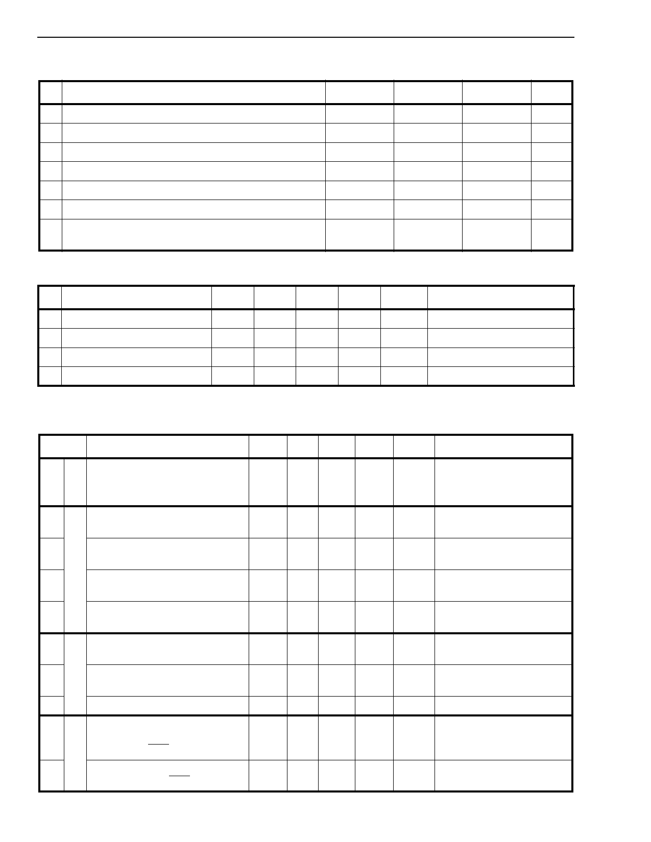
Absolute Maximum Ratings*- Voltages are with respect to ground (VSS) unless otherwise stated.
Parameter
Symbol
Min
Max
Units
1 Supply Voltage
VDD
-0.3
7.0
V
2 Voltage on any pin
VI
VSS-0.5
VDD+0.5
V
3 Input/Output Diode Current
IIK/OK
±10
mA
4 Output Source or Sink Current
IO
±25
mA
5 DC Supply or Ground Current
6 Storage Temperature
IDD/ISS
TST
-65
±50
mA
150
oC
7 Package Power Dissipation
Ceramic DIP
PD
LCC
PD
1200
600
* Exceeding these values may cause permanent damage. Functional operation under these conditions is not implied.
mW
mW
Recommended Operating Conditions - Voltages are with respect to ground (VSS) unless otherwise stated.
Characteristics
Sym Min Typ‡ Max Units
Test Conditions
1 Supply Voltage
VDD 4.75 5.0 5.25
V
2 Input HIGH Voltage
VIH
2.4
VDD
V For 400 mV noise margin
3 Input LOW Voltage
VIL
VSS
0.4
V For 400 mV noise margin
4 Operating Temperature
TA
-40
25
85
oC
‡ Typical figures are at 25°C and are for design aid only: not guaranteed and not subject to production testing.
DC Electrical Characteristics - Voltages are with respect to ground (VSS) unless otherwise stated.
VDD=5.0 V±5%; VSS=0V; TA=-40 to 85°C.
Characteristics
Sym Min Typ‡ Max Units
Test Conditions
S
1 U Supply Current
P
IDD
IDDS
8
15
mA Under clocked condition, with the
100
inputs tied to the same supply rail
as the corresponding pull-up /
down resistors.
2
Input HIGH voltage (For all the VIH 2.0
V
inputs except pin 23)
3
Positive-going threshold
I voltage (For pin 23)
4 N Input LOW voltage (For all the
inputs except pin 23)
V+ 2.8
VIL
V
0.8
V
5
Negative-going threshold
V-
voltage (For pin 23)
1.5
V
6
Output current HIGH (For all
O the outputs except pin 10)
7 U Output current LOW (For all the
T outputs except pin 10)
IOH -9.5
IOL 4.5
mA VOH=2.4 V
mA VOL=0.4 V
8
Output current LOW (pin 10)
IOL 2.0
9
Leakage current on bidirect-
IIZ/OZ
ional pins and all inputs except
C12i, C16i, RST
mA VOL=0.4 V
±150 µA VI/O=VSS or VDD
10
Leakage current on all outputs IIZ/OZ
and C12i, C16i, RST inputs
±1 ±10
µA VI/O=VSS or VDD
‡ Typical figures are at 25°C and are for design aid only: not guaranteed and not subject to production testing.
3-36
Share Link: 