IDT72511 데이터 시트보기 (PDF) - Integrated Device Technology
부품명
상세내역
일치하는 목록
IDT72511 Datasheet PDF : 28 Pages
| |||
IDT72511/IDT72521
BIDIRECTIONAL FIRST-IN FIRST-OUT MEMORY
MILITARY AND COMMERCIAL TEMPERATURE RANGES
STATE AFTER RESET
Configuration Registers 0-3
Configuration Register 4
Configuration Register 5
Configuration Register 6-7
Status Register format
B→A Read, Write, Rewrite Pointers
A→B Read, Write, Reread Pointers
DMA direction
DMA internal request
Hardware Reset
(RS asserted)
0000H
6420H
0000H
0000H
0
0
0
B→A write
clear
B→A(001)
—
—
—
—
—
0
—
—
—
Software Reset
B→A and
A→B(010) A→B(011)
Internal
Request
(100)
—
—
—
—
—
—
—
—
—
—
—
—
—
—
—
—
0
—
0
0
—
—
—
—
—
—
clear
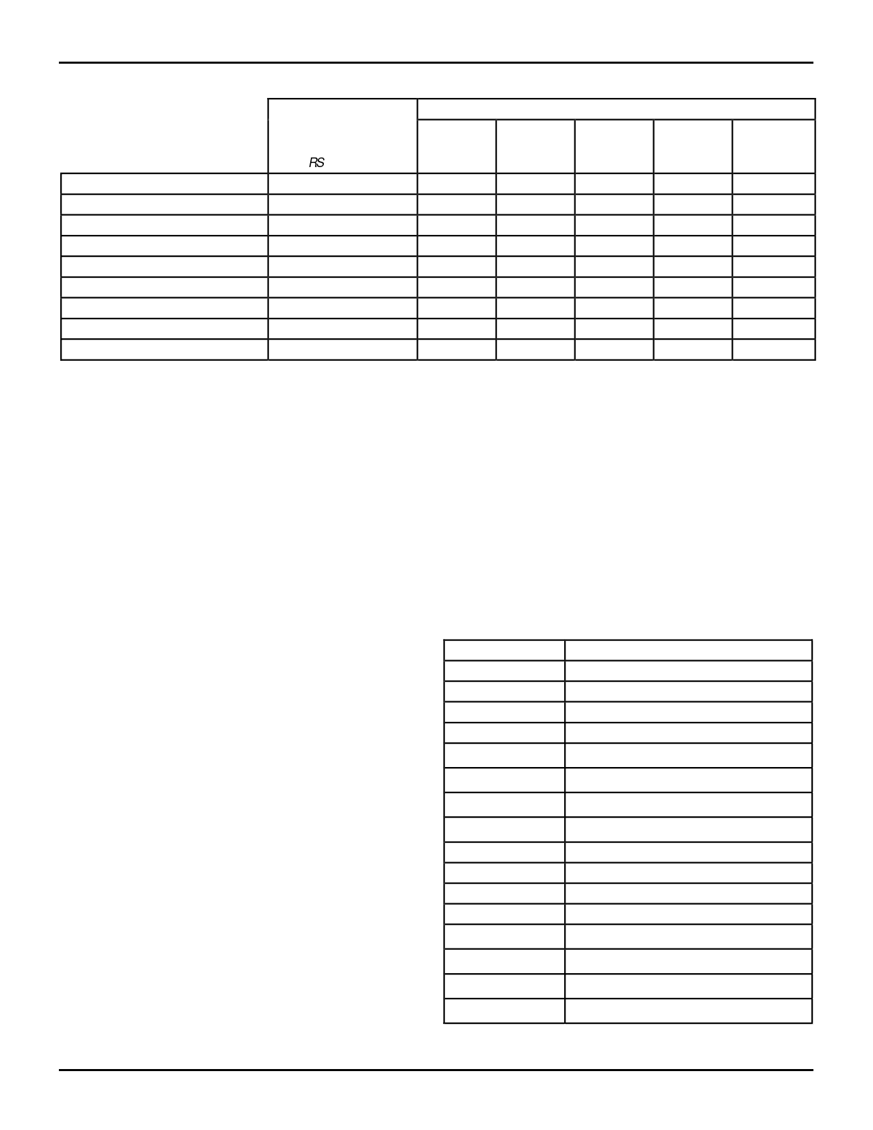
Table 6. The BiFIFO State After a Reset Command
All(111)
0000H
6420H
0000H
0000H
—
0
0
—
clear
2668 tbl 08
Table 8. Configuration Registers 0-3 contain the programmable
flag offsets for the Almost-Empty and Almost-Full flags. These
offsets are set to 0 when a hardware reset or a software Reset
All is applied. Note that Table 8 shows that Configuration
Registers 0-3 are 10 bits wide to accommodate the 1024
locations in each FIFO memory of the IDT7252/520. Only 9
least significant bits are used for the 512 locations of the
IDT7251/510; the most significant bit, bit 9, must be set to 0.
Configuration Register 4 is used to assign the internal flags
to the external flag pins (FLGA-FLGD). Each external flag pin
is assigned an internal flag based on the four bit codes shown
in Table 9. The default condition for Configuration Register 4
is 6420H as shown in Table 6. The default flag assignments
are: FLGD is assigned B→A Full, FLGC is assigned B→A
Empty, FLGB is assigned A→B Full, FLGA is assigned A→B
Empty.
Configuration Register 5 is a general control register. The
format of Configuration Register 5 is shown in Table 10.
Bit 0 sets the Intel-style interface (RB, WB) or Motorola-style
interface (DSB, R/WB) for Port B. Bits 2 and 3 redefine Full and
Empty Flags for reread/rewrite data protection.
Bits 4-9 control the DMA interface and are only applicable
in peripheral interface mode. In processor interface mode,
these bits are don’t care states. Bits 4 and 5 set the polarity of
the DMA control pins REQ and ACK respectively. An internal
clock controls all DMA operations. This internal clock is
derived from the external clock (CLK). Bit 9 determines the
internal clock frequency: the internal clock = CLK or the
internal clock = CLK divided by 2. Bit 8 sets whether RB, WB,
and DSB are asserted for either one or two internal clocks. Bits
6 and 7 set the number of internal clocks between REQ
assertion and ACK assertion. The timing can be from 2 to 5
cycles as shown in Figure 17.
Bit 10 controls Port B processor or peripheral interface
mode. In processor mode, the Port B control pins (RB, WB,
DSB, R/WB) are inputs and the DMA controls are ignored. In
peripheral mode, the Port B control pins are outputs and the
DMA controls are active.
Six PIO pins can be programmed as an input or output
by the corresponding mask bits in Configuration Register 7.
The format of Configuration Register 7 is shown in Figure
5. Each bit of the register set the I/O direction independ-
ently. A logic 1 indicates that the corresponding PIO pin is
an output, while a logic 0 indicates that the PIO pin is an
input. This I/O mask register can be read or written.
A programmed output PIOi pin (i = 0, 1, . . . 5) displays the
data latched in Bit i of Configuration Register 6. A programmed
input PIOi pin allows Port A bus to sample the data on DAi by
reading Configuration Register 6.
STATUS REGISTER FORMAT
Bit
Signal
0
Reserved
1
Reserved
2
Reserved
3
DMA Direction
4
A→B Empty Flag
5
A→B Almost-Empty Flag
6
B→A Full Flag
7
B→A Almost-Full Flag
8
Reserved
9
Reserved
10
Reserved
11
Reserved
12
A→B Full Flag
13
A→B Almost-Full Flag
14
B→A Empty Flag
15
B→A Almost-Empty Flag
Table 7. The Status Register Format
2668 tbl 09
5.32
9
Share Link: 