IDT72511 데이터 시트보기 (PDF) - Integrated Device Technology
부품명
상세내역
일치하는 목록
IDT72511 Datasheet PDF : 28 Pages
| |||
IDT72511/IDT72521
BIDIRECTIONAL FIRST-IN FIRST-OUT MEMORY
MILITARY AND COMMERCIAL TEMPERATURE RANGES
Peripheral Interface Mode
If Port B is connected to a peripheral controller, all
BiFIFOs in the configuration must be programmed in peri-
pheral interface mode. In this mode, all the Port B interface
pins are all outputs. To assure fixed high states for RB and
WB before they are programmed into an output, these two
pins should be pulled up to VCC with 10K resistors. Of
course, only one set of Port B interface pins should be used
to control a single peripheral device, while the other interface
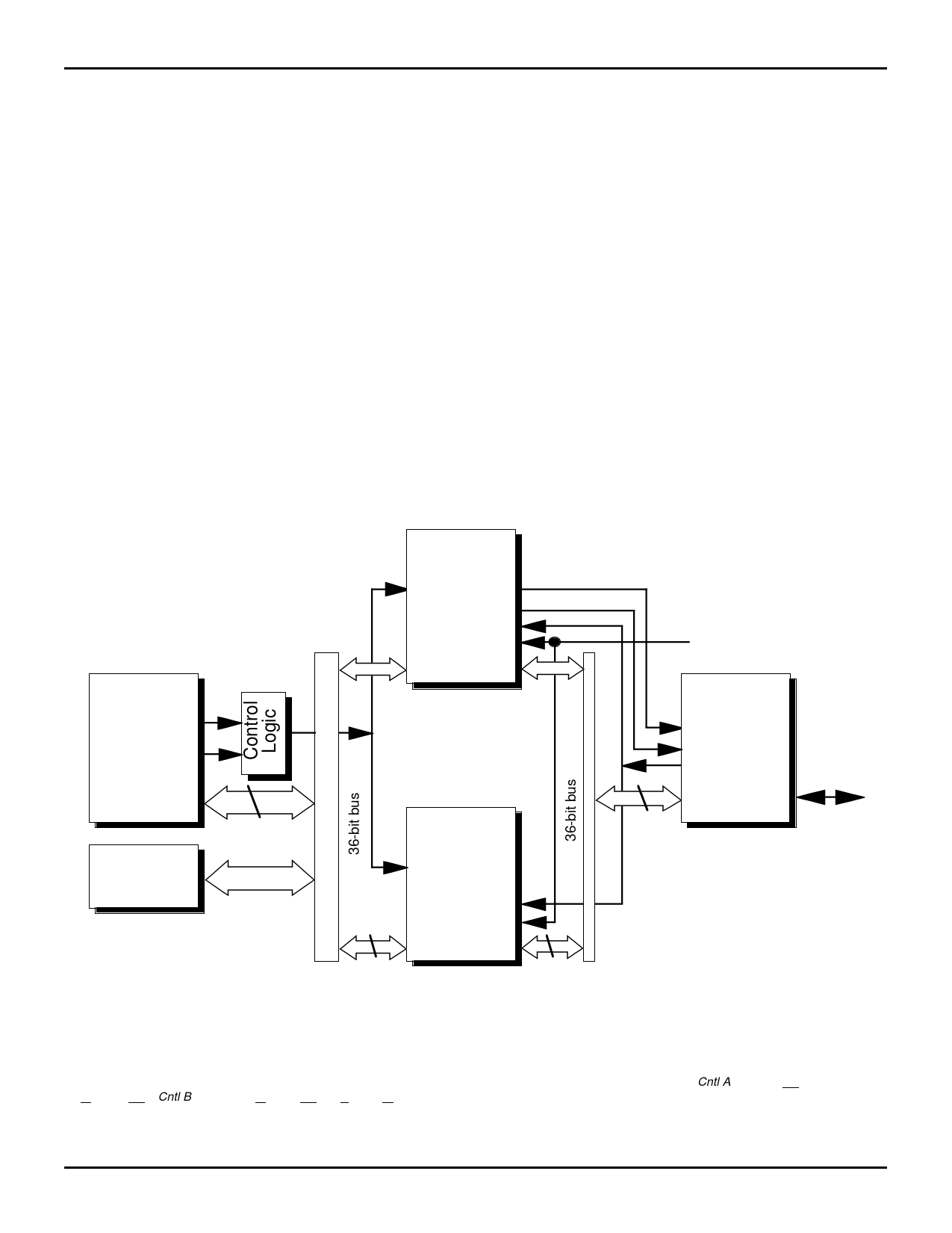
pins are all ignored. Figure 2 shows a BiFIFO configuration
connected to a peripheral.
Port A Interface
The BiFIFO is straightforward to use in microprocessor-
based systems because each BiFIFO port has a standard
microprocessor control set. Port A has access to six re-
sources: the A→B FIFO, the B→A FIFO, the 9-bit direct data
bus (bypass path), the configuration registers, status and
command registers. The Port A Address and Read/Write
pins determine the resource being accessed as shown in
Table 1. Data Strobe is used to move data in and out of the
BiFIFO.
When either of the internal FIFOs are accessed, 18 bits of
data are transferred across Port A. Since the bypass path is
only 9 bits wide, the least significant byte (DA0-DA7, DA16) is
used on Port A. All of the registers are 16 bits wide which
means only the data bits (DA0-DA15) are passed by Port A.
Bypass Path
The bypass path acts as a bidirectional bus transceiver
directly between Port A and Port B. The direct connection
requires that the Port A interface pins are inputs and the Port
B interface pins are outputs. The bypass path is 9 bits wide in
an 18- to 18-bit configuration or 18 bits wide in a 36- to 36-
bit configuration.
During bypass operations, the BiFIFOs must be pro-
grammed into peripheral interface mode. Bit 10 of Configura-
tion Register 5 (see Table 10) is set to 1 for peripheral
interface mode.
Command Register
Ten registers are accessible through Port A, a Command
Register, a Status Register, and eight Configuration
Registers.
Processor
Address
Control
Data
36
RAM
IDT
BiFIFO
Cntl A
Cntl B
ACK
REQ
CLK
Data A Data B
IDT
BiFIFO
Cntl Cntl B
A
ACK
REQ
CLK
Data A Data B
18
18
DMA or System
Clock
Peripheral
Controller
Cntl
ACK
REQ
Data
I/O
Data
36
2668 drw 06
Figure 2. 36-Bit Processor to 36-Bit Peripheral Configuration
NOTE:
1. 36- to 36-bit peripheral interface configuration. Upper BiFIFO only is used in 18- to 18-bit configuration. Note that Cntl A refers to CSA, A1, A0, R/
WA, and DSA; Cntl B refers to R/WB and DSB or RB and WB.
5.32
6
Share Link: 