CS8361 데이터 시트보기 (PDF) - ON Semiconductor
부품명
상세내역
일치하는 목록
CS8361 Datasheet PDF : 8 Pages
| |||
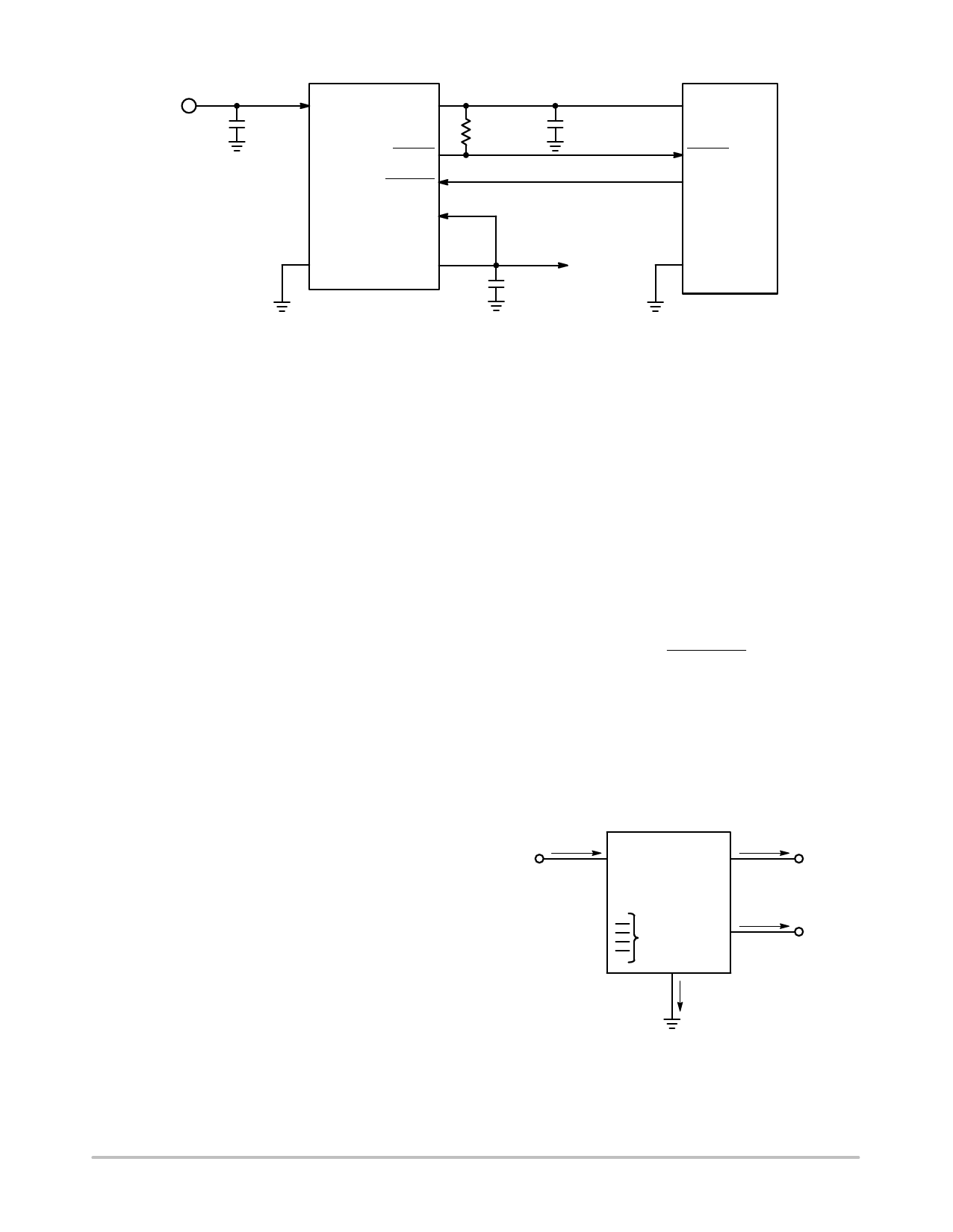
CS8361
5.0 V, 100 mA
B+
C1*
VIN
VSTBY
C2**
VDD
0.1 mF
CS8361
R3
10 mF
MCU
RESET
ESR < 8.0 W
RESET
ENABLE
I/O
Adj
GND
VTRK
SW 5.0 V,
C3**
250 mA
10 mF
ESR < 8.0 W
GND
*C1 is required if regulator is located far from power supply filter.
**C2 and C3 are required for stability.
Figure 3. Test and Application Circuit, Dual 5.0 V Regulator
APPLICATION NOTES
External Capacitors
Output capacitors for the CS8361 are required for
stability. Without them, the regulator outputs will oscillate.
Actual size and type may vary depending upon the
application load and temperature range. Capacitor effective
series resistance (ESR) is also a factor in the IC stability.
Worst−case is determined at the minimum ambient
temperature and maximum load expected.
Output capacitors can be increased in size to any desired
value above the minimum. One possible purpose of this
would be to maintain the output voltages during brief
conditions of negative input transients that might be
characteristic of a particular system.
Capacitors must also be rated at all ambient temperatures
expected in the system. To maintain regulator stability down
to −40°C, capacitors rated at that temperature must be used.
More information on capacitor selection for SMART
REGULATOR®s is available in the SMART REGULATOR
application note, “Compensation for Linear Regulators,”
document number SR003AN/D, available through the
Literature Distribution Center or via our website at
http://www.onsemi.com.
Calculating Power Dissipation in a
Dual Output Linear Regulator
The maximum power dissipation for a dual output
regulator (Figure 4) is
PD(max) + NJVIN(max) * VOUT1(min)NjIOUT1(max) )
NJVIN(max) * VOUT2(min)NjIOUT2(max) ) VIN(max)IQ (1)
IOUT1(max) is the maximum output current, for the
application,
IOUT2(max) is the maximum output current, for the
application, and
IQ is the quiescent current the regulator consumes at both
IOUT1(max) and IOUT2(max).
Once the value of PD(max) is known, the maximum
permissible value of RqJA can be calculated:
RQJA
+
150°
C*
PD
TA
(2)
The value of RqJA can be compared with those in the
package section of the data sheet. Those packages with
RqJA’s less than the calculated value in equation 2 will keep
the die temperature below 150°C.
In some cases, none of the packages will be sufficient to
dissipate the heat generated by the IC, and an external
heatsink will be required.
IIN
VIN
SMART
REGULATOR
IOUT1
VOUT1
Control
Features
IOUT2
VOUT2
IQ
where:
VIN(max) is the maximum input voltage,
VOUT1(min) is the minimum output voltage from VOUT1,
VOUT2(min) is the minimum output voltage from VOUT2,
Figure 4. Dual Output Regulator With Key
Performance Parameters Labeled.
http://onsemi.com
5
Share Link: 