CS8361 데이터 시트보기 (PDF) - ON Semiconductor
부품명
상세내역
일치하는 목록
CS8361 Datasheet PDF : 8 Pages
| |||
CS8361
PACKAGE PIN DESCRIPTION
PACKAGE PIN #
D2PAK, 7 Pin
SO−16L
1
16
2
1
3
3
4
4, 5, 12, 13
5
6
6
8
7
9
2, 7, 10, 11,
14, 15
PIN SYMBOL
VSTBY
VIN
VTRK
GND
Adj
ENABLE
RESET
NC
FUNCTION
Standby output voltage delivering 100 mA.
Input voltage.
Tracking output voltage controlled by ENABLE delivering 250 mA.
Reference ground connection.
Resistor divider from VTRK to Adj. Sets the output voltage on
VTRK. If tied to VTRK, VTRK will track VSTBY.
Provides on/off control of the tracking output, active LOW.
CMOS compatible output lead that goes low whenever VSTBY falls
out of regulation.
No connection.
CIRCUIT DESCRIPTION
ENABLE Function
The ENABLE function switches the output transistor for
VTRK on and off. When the ENABLE lead voltage exceeds
1.4 V (Typ), VTRK turns off. This input has several hundred
millivolts of hysteresis to prevent spurious output activity
during power−up or power−down.
RESET Function
The RESET is an open collector NPN transistor,
controlled by a low voltage detection circuit sensing the
VSTBY (5.0 V) output voltage. This circuit guarantees the
RESET output stays below 1.0 V (0.1 V Typ) when VSTBY
is as low as 1.0 V to ensure reliable operation of
microprocessor− based systems.
VTRK Output Voltage
This output uses the same type of output device as VSTBY,
but is rated for 250 mA. The output is configured as a
tracking regulator of the standby output. By using the
standby output as a voltage reference, giving the user an
external programming lead (Adj lead), output voltages from
5.0 V to 20 V are easily realized. The programming is done
with a simple resistor divider (Figure 2), and following the
formula:
VTRK + VSTBY (1 ) R1ńR2) ) IAdj R1
If another 5.0 V output is needed, simply connect the Adj
lead to the VTRK output lead.
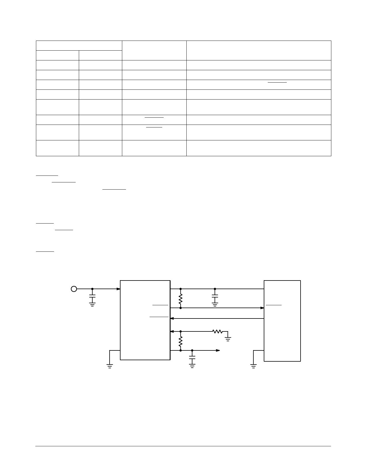
5.0 V, 100 mA
B+
C1*
VIN
VSTBY
C2**
VDD
0.1 mF
CS8361
R3
10 mF
MCU
RESET
ESR < 8.0 W
RESET
ENABLE
Adj
I/O
R2
GND
VTRK
R1
SW 8.0 V,
C3**
250 mA
10 mF
ESR < 8.0 W
GND
VTRK ∼ VSTBY(1 + R1/R2)
For VTRK ∼ 8.0 V, R1/R2 ∼ 0.6
*C1 is required if regulator is located far from power supply filter.
**C2 and C3 are required for stability.
Figure 2. Test and Application Circuit, 5.0 V, 8.0 V Regulator
http://onsemi.com
4
Share Link: 