CS8361 데이터 시트보기 (PDF) - ON Semiconductor
부품명
상세내역
일치하는 목록
CS8361 Datasheet PDF : 8 Pages
| |||
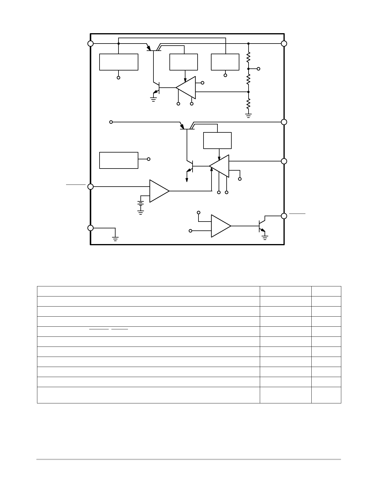
CS8361
VIN
Overvoltage
Shutdown
OVSD
VIN
ENABLE
Thermal
Shutdown
GND
Current
Limit
+
−
Bandgap
BG BG
TSD OVSD
Current
Limit
TSD
−
+
−
VSTBY
+
TSD OVSD
BG
+
RESET
−
VSTBY
5.0 V, 100 mA, 2.0%
RESET
VTRK
250 mA
Adj
RESET
Figure 1. Block Diagram. Consult Your Local Sales Representative for Positive ENABLE Option
MAXIMUM RATINGS*
Rating
Value
Unit
Supply Voltage, VIN
Positive Transient Input Voltage, tr > 1.0 ms
−16 to 26
V
60
V
Negative Transient Input Voltage, T < 100 ms, 1.0 % Duty Cycle
−50
V
Input Voltage Range (ENABLE, RESET)
−0.3 to 10
V
Tracking Regulator (VTRK, Adj)
Standby Regulator (VSTBY)
Junction Temperature
20
V
10
V
−40 to +150
°C
Storage Temperature Range
−55 to +150
°C
ESD Susceptibility (Human Body Model)
2.0
kV
Lead Temperature Soldering
Wave Solder (through hole styles only) Note 1
260 peak
°C
Reflow (SMD styles only) Note 2
230 peak
°C
Maximum ratings are those values beyond which device damage can occur. Maximum ratings applied to the device are individual stress limit
values (not normal operating conditions) and are not valid simultaneously. If these limits are exceeded, device functional operation is not implied,
damage may occur and reliability may be affected.
1. 10 seconds max.
2. 60 seconds max above 183°C
*The maximum package power dissipation must be observed.
http://onsemi.com
2
Share Link: 