NJU6635CH 데이터 시트보기 (PDF) - Japan Radio Corporation
부품명
상세내역
일치하는 목록
NJU6635CH Datasheet PDF : 33 Pages
| |||
NJU6635
(1-6)Character Generator RAM
The character generator RAM (CG RAM) stores any kinds of character pattern in 5 x 8 dots written by
the user program to display user’s original character pattern. The CG RAM stores 4 kinds of character
in 5 x 8 dots mode.
To display user’s original character pattern stored in the CG RAM, the address data (00)H – (03)H
should be written to the DD RAM as shown in Table 2.
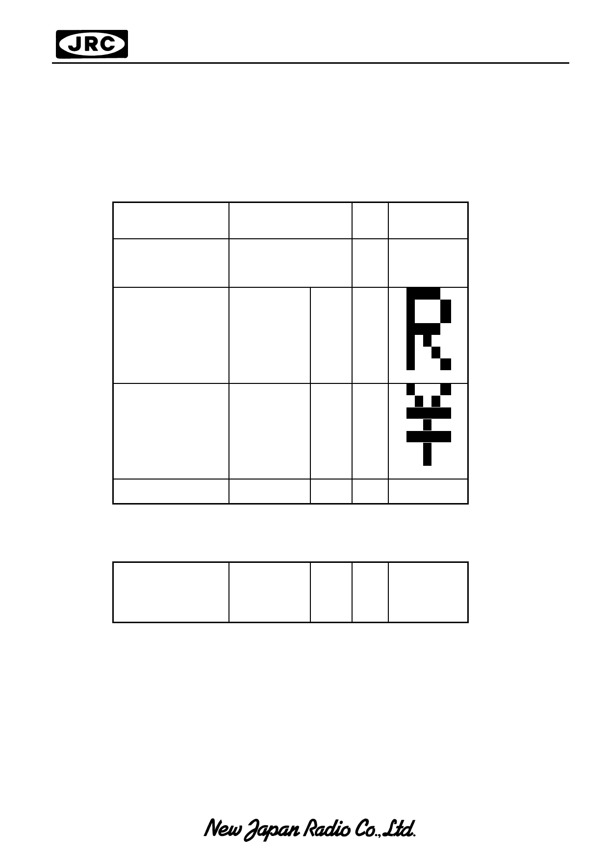
Table 3. shows the correspondence among the character pattern, CG RAM address and data.
Table 3. Correspondence of CG RAM address, DD RAM character code
and CG RAM character pattern (5 x 8 dots)
Character Code
(DD RAM Data)
CG RAM Address
Character
Pattern
(CG RAM Data)
76543210
←
→
Upper bit Lower bit
←
Upper bit
43 210
→
Lower bit
43210
←
→
Upper Lower
bit
bit
000
11110
001
10001
010
10001
Character
0000∗∗00
00 0 1 1
100
11110
10100
Pattern
Example (1)
101
10010
110
10001
111
0 0 0 0 0 ←Cursor Position
000
10001
001
01010
010
11111
Character
0000∗∗01
01 011
100
00100
11111
Pattern
Example (2)
101
110
00100
00100
111
0 0 0 0 0 ← Cursor Position
000
001
!
!
!
!
!
!
!
!
!
!
!
!
!
!
!
!
!
!
!
!
0000∗∗11
11
100
101
110
111
Notes: 1. Character code bits 0 and 1 correspond to the CG RAM address 3 and 4 ( 2bits : 4 patterns).
2. CG RAM address 0, 1 and 2 designate a character pattern line position.
The 8th line is the cursor position and the display is performed by logical OR with cursor.
Therefore, in case of the cursor display, the data of 8th line should be “0”.
If there is “1” in the 8th line, the bit “1” is always displayed on the cursor position regardless of
cursor existence.
3. Character pattern row position corresponding to the CG RAM data bits 0 to 4 are all shown above.
The bits 5 to 7 of the CG RAM do not exist.
4. CG RAM character patterns are selected when character code bits 4 to 7 are all “0” and addressed
by character code bits 0 and 1. Therefore the address (00)H, (04)H, (08)H and (0C)H, select the
same character pattern as shown In table 2 and Table 3.
5. ”1” for CG RAM data corresponds to display On and “0” to display Off.
Share Link: 