NJU6635CH 데이터 시트보기 (PDF) - Japan Radio Corporation
부품명
상세내역
일치하는 목록
NJU6635CH Datasheet PDF : 33 Pages
| |||
NJU6635
s FUNCTIONAL DESCRIPTION
(1)Description for each blocks
(1-1)Register
The NJU6635 incorporates two 8-bit registers, an Instruction Register (IR) and a Data Register (DR).
The Register (IR) stores Instruction codes such as “Clear Display” and “Return Home”, and address
data for Display Data RAM (DD RAM) and Character Generator RAM (CG RAM). The MPU can write
the Instruction code and address data to the Register (IR), but it can not read out from the Register (IR).
The Register (DR) is a temporary storing register, the data in the Register (DR) is written into the DD
RAM or CG RAM and read out from the DD RAM or CG RAM.
The data in the Register (DR) written by the MPU is transferred from the Register automatically to the
DD RAM or CG RAM by Internal operation.
After reading the data in the Register (DR) by the MPU, the next address data in the DD RAM or CG
RAM is transferred automatically to the Register (DR) for the next MPU reading.
These two registers are selected by the selection signal RS as shown below:
Table 1. Register operation control by RS and R/W signals.
Table 1. Register Operation
RS R/W
Operation
0
0 Write
0
1 Read busy flag (DB7) and address counter (DB0 to DB7)
1
0 Write (DR to DD or CG RAM)
1
1 Read (DD or CG RAM to DR)
(1-2)Busy Flag (BF)
When the internal circuits are operating, the busy flag is “1”, and any instruction reading is inhibited.
The busy flag (BF) is output from DB7 when RS=”0” and R/W=”1” as shown in table 1.
The next instruction should be written after busy flag (BF) goes to “0”.
(1-3)Address Counter(AC)
The address Counter (AC) addresses the DD RAM and CG RAM.
When the address setting instruction is written into the Register (IR), the address information is
transferred from Register (IR) to the counter (AC). The selection of either the DD RAM or CG RAM is
also determined by this instruction.
After writing (or reading) the display data to (or from) the DD RAM or CG RAM, the counter (AC)
increments (or decrements) “1” automatically.
The address data in the Counter (AC) is output from DB6 to DB0 when RS=”0” and R/W=”1” as shown
in table 1.
(1-4)Display Data RAM (DD RAM)
The display data RAM (DD RAM) consisting of 32 x 8 bits stores up to 32-character display data
represented in 8-bit code.
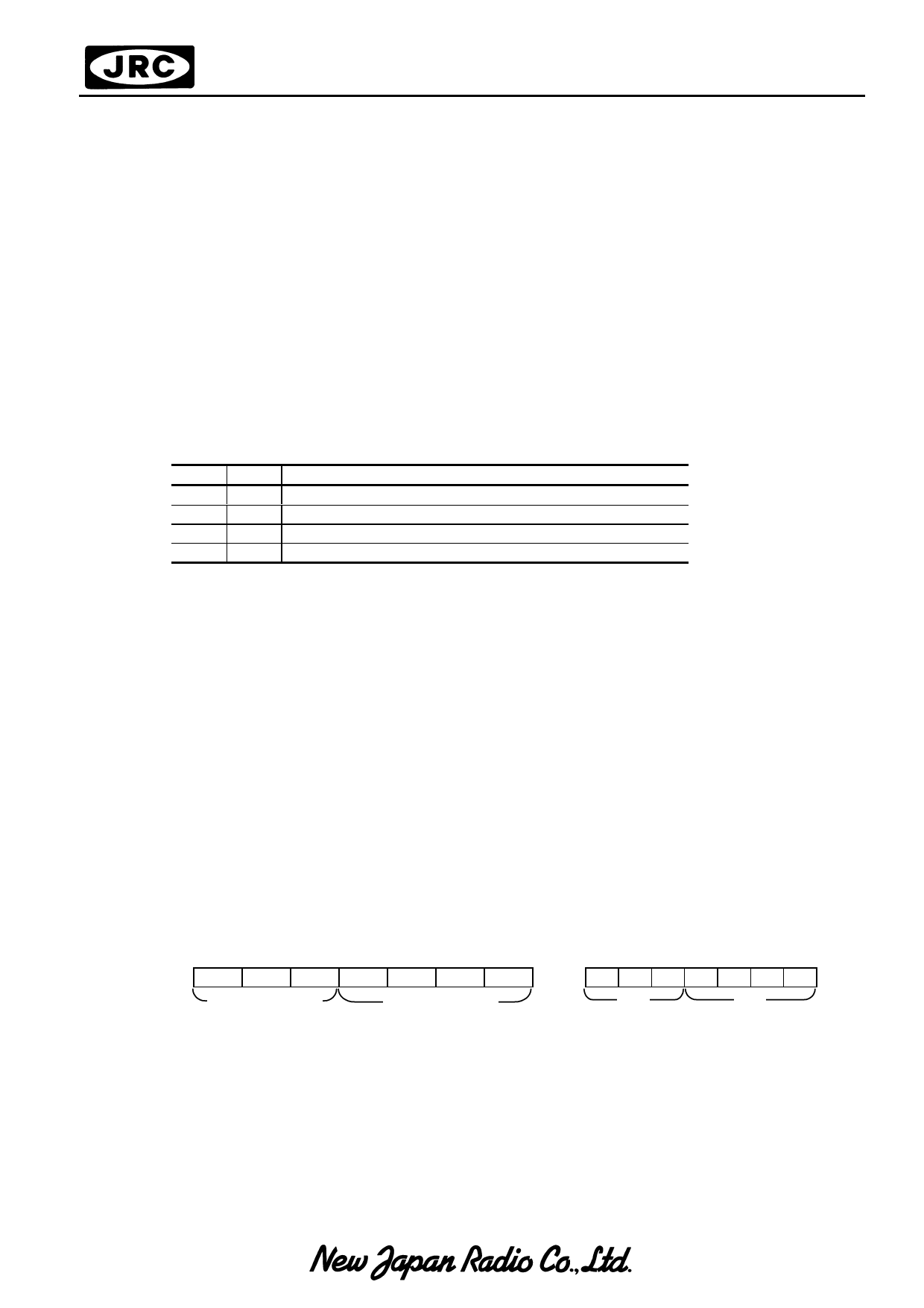
The DD RAM address data set in the address Counter (AC) is represented in hexadecimal.
←Higher order bit
Lower order bit→
AC AC6 AC5 AC4 AC3 AC2 AC1 AC0
Hexadecimal
Hexadecimal
(Example) DD RAM address “ 08 ”
0001000
0
8
Share Link: 