NJU6635CH 데이터 시트보기 (PDF) - Japan Radio Corporation
부품명
상세내역
일치하는 목록
NJU6635CH Datasheet PDF : 33 Pages
| |||
NJU6635
(1-7)Timing Generator
The timing generator generates a timing signals for the DD RAM, CG RAM, CG ROM and other
internal circuit operation.
RAM read timing for the display and internal operation timing for MPU access are separately
generated, so that they may not interfere with each other.
Therefore, when the data write to the DD RAM for example, there will be undesirable Influence, such
as flickering, in areas other than the display area.
(1-8)LCD Driver
LCD driver consists of 16-common driver and 80-segment driver.
The 80 bits of character pattern data are shifted in the shift-register and latched when the 40 bits shift
performed completely. This latched data controls display driver to output LCD driving waveform.
(1-9)Cursor Blinking Control Circuit
This circuits controls cursor On/Off and cursor position character blinks. The cursor or blinks
appears in the digit position at the DD RAM address set in the address counter(AC).
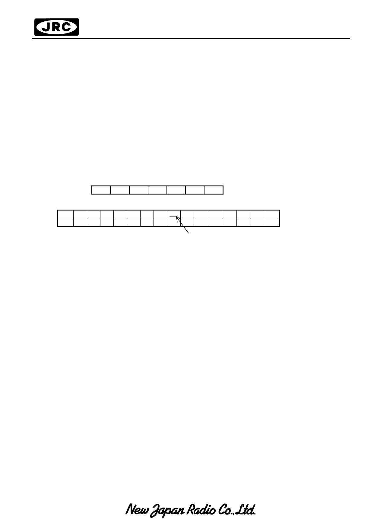
When the address counter is (08)H, a cursor position is shown as follows:
AC6 AC5 AC4 AC3 AC2 AC1 AC0
AC 0 0 0 1 0 0 0
1
1st line 00
2nd line 10
2 3 4 5 6 7 8 9 10 11 12 13 14 15 16 ← Display Position
01 02 03 04 05 06 07 08 09 0A 0B 0C 0D 0E 0F ← DD RAM Address
11 12 13 14 15 16 17 18 19 1A 1B 1C 1D 1E 1F
(Hexadecimal)
Cursor Position
Note) The cursor or blinks appears when the address counter (AC) selects the CG RAM.
But the displayed cursor and blink are meaningless.
If the AC stores the CG RAM address data, the cursor and blink are displayed in the meaningless
position.
Share Link: 