7641 데이터 시트보기 (PDF) - Mitsumi
부품명
상세내역
일치하는 목록
7641 Datasheet PDF : 149 Pages
| |||
PRELIMINARY NSocothimcaene:gpTeah.riasmisetnrioct laimfiintsalasrepescuibfijceacttioton.
MITSUBISHI MICROCOMPUTERS
7641 Group
SINGLE-CHIP 8-BIT CMOS MICROCOMPUTER
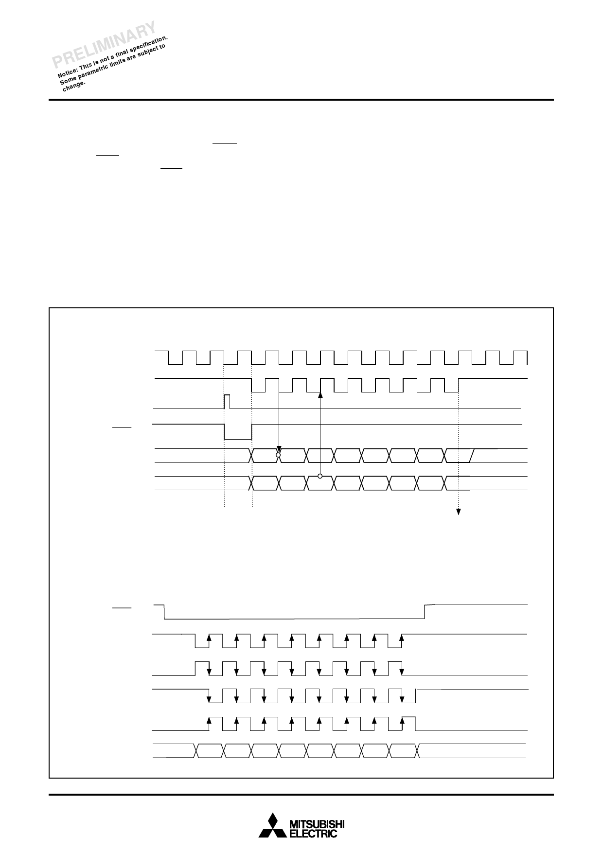
Serial I/O Normal Operation
The serial I/O counter is set to “7” by writing operation to the serial
I/O shift register (address 002A16). When the SRDY Output Select
bit is “1”, the SRDY pin goes “L” after that writing. On the negative
edge of the transfer clock the SRDY pin returns “H” and the data
of the first bit is transmitted from the STXD pin. The remaining
data are done from the STXD pin bit by bit on each falling edge of
the transfer clock.
Additionally, the data is latched from the SRXD pin on each rising
edge of the transfer clock and then the contents of the serial I/O
shift register are shifted by one bit.
When the internal system clock is selected as the transfer clock,
the followings occur at counting eight transfer clocks:
•The serial I/O counter reaches “0”
•The transfer clock halts at “H”
•The serial I/O interrupt request bit is set to “1”
•The STXD pin goes a high-impedance state after an 8-bit transfer
is completed.
When the external clock is selected as the transfer clock, the fol-
lowings occur at counting eight transfer clocks:
•The serial I/O counter reaches “0”
•The serial I/O interrupt request bit is set to “1”
In this case, the transfer clock needs to be controlled by the exter-
nal source because the transfer clock does not halt. Additionally,
the STXD pin does not go a high-impedance state after an 8-bit
transfer is completed.
Figure 25 shows serial I/O timing.
qNormal mode timing (LSB first)
Synchronizing clock
Transfer clock
Serial I/O shift
register write signal
SRDY signal
Serial I/O output STXD
Serial I/O input SRXD
D0
D1 D2
D3
D4
D5
D6
(Note)
D7
Interrupt request bit is set to “1”.
Note: When the internal clock is selected as the transfer clock, the STXD pin goes to a high-impedance state after transfer completion.
qSPI compatible mode timing
SRDY signal
Synchronizing clock
SCLK (CPoL = 1, CPha =1 )
SCLK (CPoL = 0, CPha = 1)
SCLK (CPoL = 1, CPha = 0)
SCLK (CPoL = 0, CPha = 0)
STXD/SRXD
First
Fig. 25 Serial I/O timing
Last
30
Share Link: 