7641 데이터 시트보기 (PDF) - Mitsumi
부품명
상세내역
일치하는 목록
7641 Datasheet PDF : 149 Pages
| |||
PRELIMINARY NSocothimcaene:gpTeah.riasmisetnrioct laimfiintsalasrepescuibfijceacttioton.
MITSUBISHI MICROCOMPUTERS
7641 Group
SINGLE-CHIP 8-BIT CMOS MICROCOMPUTER
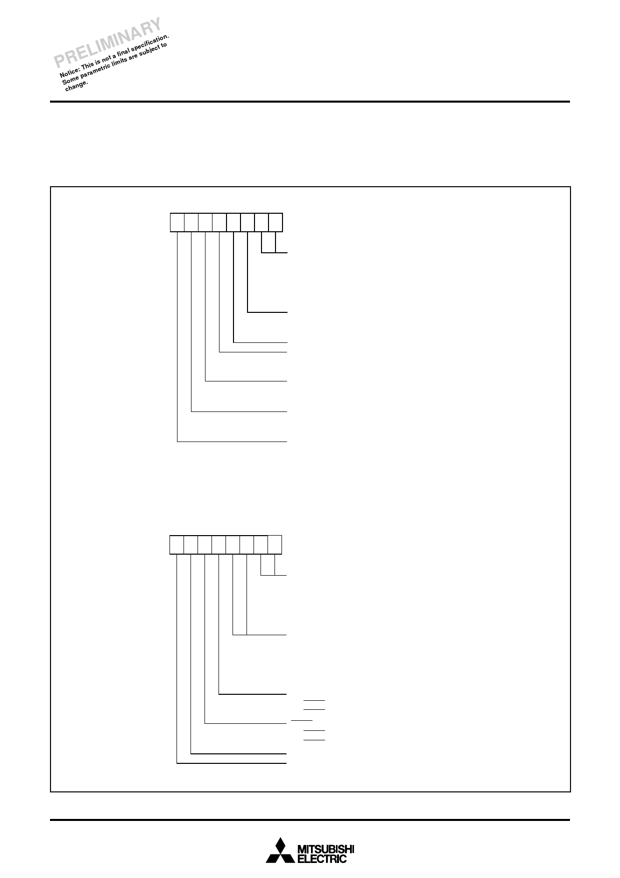
[CPU Mode Registers A, B (CPUMA, CPUMB)] 000016, 000116
The CPU mode register contains the stack page select bit and the
CPU operating mode select bit and so on.
The CPU mode registers are allocated at address 000016, 000116.
s Notes
Do not use the microprocessor mode in the flash memory version.
b7
b0
1
CPU mode register A (address 000016)
CPMA
Processor mode bits
b1b0
0 0: Single-chip mode
0 1: Memory expansion mode
1 0: Microprocessor mode (Note 1)
1 1: Not available
Stack page select bit
0: Page 0
1: Page 1
Fix to “1”.
Sub-clock (XCIN-XCOUT) stop bit
0: Oscillating
1: Stopped
Main clock (XIN-XOUT) stop bit
0: Oscillating
1: Stopped
Internal system clock select bit (Note 2)
0: External clock (XIN-XOUT or XCIN-XCOUT)
1: fSYN
External clock select bit
0: XIN-XOUT
1: XCIN-XCOUT
Notes 1: This is not available in the flash memory version.
2: When (CPMA 6, 7) = (0, 0), the internal system clock can be selected
between f(XIN) or f(XIN)/2 by CCR7.
The internal clock φ is the internal system clock divided by 2.
b7
10
b0
CPU mode register B (address 000116)
CPMB
Slow memory wait select bits
b1b0
0 0: No wait
0 1: One-time wait
1 0: Two-time wait
1 1: Three-time wait
Slow memory wait mode select bits
b3b2
0 0: Software wait
0 1: Not available
1 0: RDY wait
1 1: Software wait plus RDY input anytime wait
Expanded data memory access bit
0: EDMA output disabled
1: EDMA output enabled
HOLD function enable bit
0: HOLD function disabled
1: HOLD function enabled
Resereved bit (“0” at read/write)
Fix to “1”.
Fig. 8 Structure of CPU mode register
11
Share Link: 