MP3274 데이터 시트보기 (PDF) - Exar Corporation
부품명
상세내역
일치하는 목록
MP3274 Datasheet PDF : 16 Pages
| |||
DB N
3k
CL
a. High-Z to VON
DB N
+5 V
3k
CL
b. High-Z to VOL
Figure 3. Load Circuit for Data
Access Time Test
DB N
3k
10pF
MP3274
DB N
+5 V
3k
10pF
a. VON to High-Z
b. VOL to High-Z
Figure 4. Load Circuit for
Bus Relinquish Time Test
STL, STS
CL
DGND
Figure 5. Load Circuit for WR to STS Delay
Serial Data Output Mode (PXS = 0)
The MP3274 output data is available in serial form when PXS
= 0 prior to the RD high-to-low transition. When PXS = 0, the
DB11/SDO pin functions as the serial data output. The
DB0/SDC pin functions as the serial clock input and all other
data outputs are 3-stated.
The serial data output sequence is MSB (DB11) first to LSB
(DB0) last. The MSB (DB11) data bit appears at DB11/SDO
when STS goes low. The second most significant bit appears at
DB11/SDO on the next DB0/SDC high-to-low transition. The
LSB (DB0) is present at DB11/SDO on the 11th SDC high-to-low
transition.
The control pin functions (ADEN, CS, WR, and RD) are the
same as the parallel mode of operation. Further information re-
garding serial control and timing is shown in Figure 6., Table 4.
and Table 5.
For a minimum interconnect serial environment, the channel
address state can be generated in at least two ways, using an
address counter, or using an address serial to parallel converter.
WR can then be used as the counter clock or shift register load
signal as well as the A/D converter start convert signal on the ris-
ing edge. (Note that the falling edge loads the address present at
the address port.)
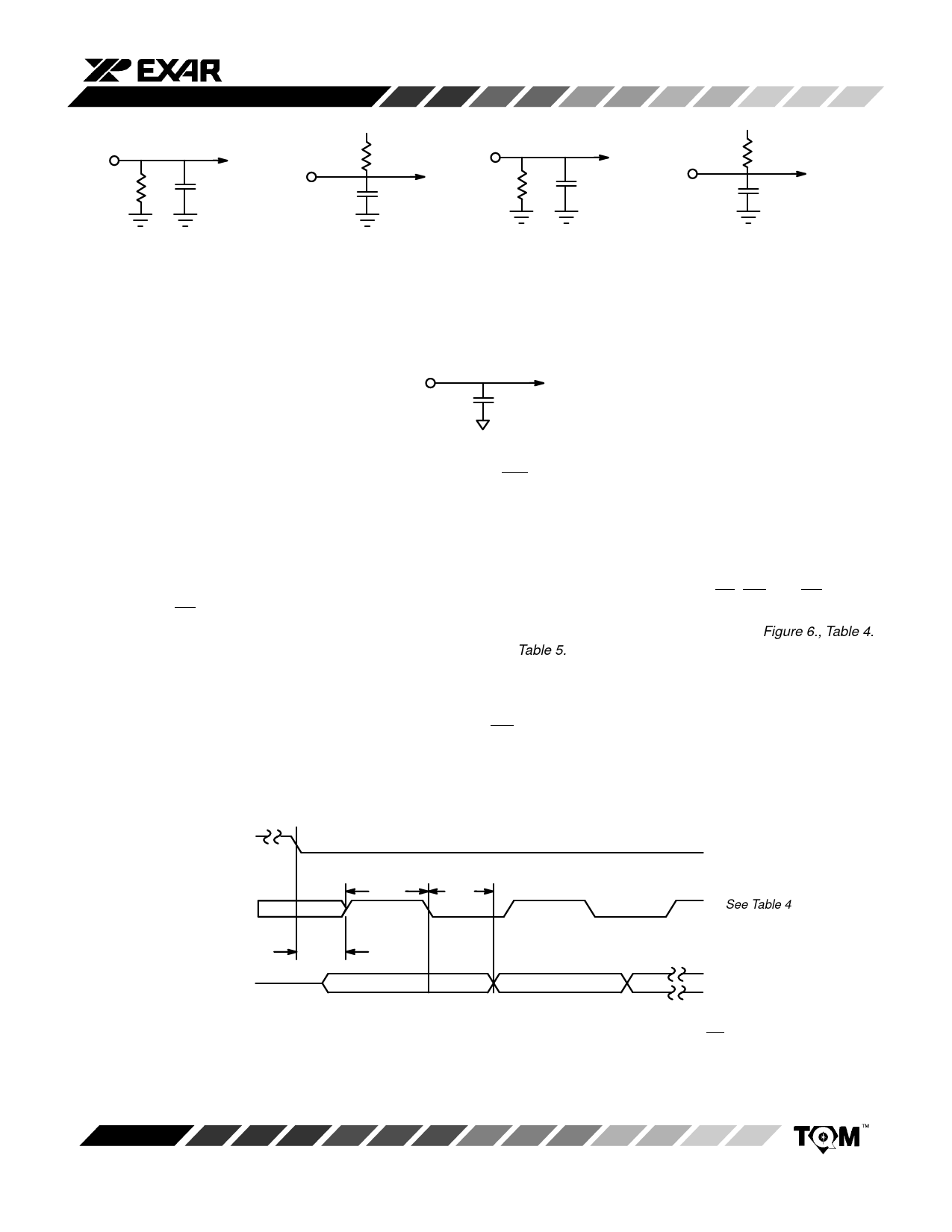
STS
SDCÇÇÇÇÇÇÇÇÇÇ t21
t22
DB11/SDO
t20
DB11 (MSB)
DB10
See Table 4
SDC should be in a high state during the STS high period. SDC can make the first high to low transition after t21. In normal use it is
assumed that PXS is hardwired low. However, if the mode of operation is changed, PXS must go low prior to RD going low.
Figure 6. Serial Data Mode Timing
Rev. 4.00
9
Share Link: 