MP3274 데이터 시트보기 (PDF) - Exar Corporation
부품명
상세내역
일치하는 목록
MP3274 Datasheet PDF : 16 Pages
| |||
MP3274
The MP3274 is easily interfaced to a wide variety of micropro-
cessors and other digital systems. Discussion of the timing re-
quirements of the MP3274 control signals will provide the sys-
tem designer with useful insight into the operation of the device.
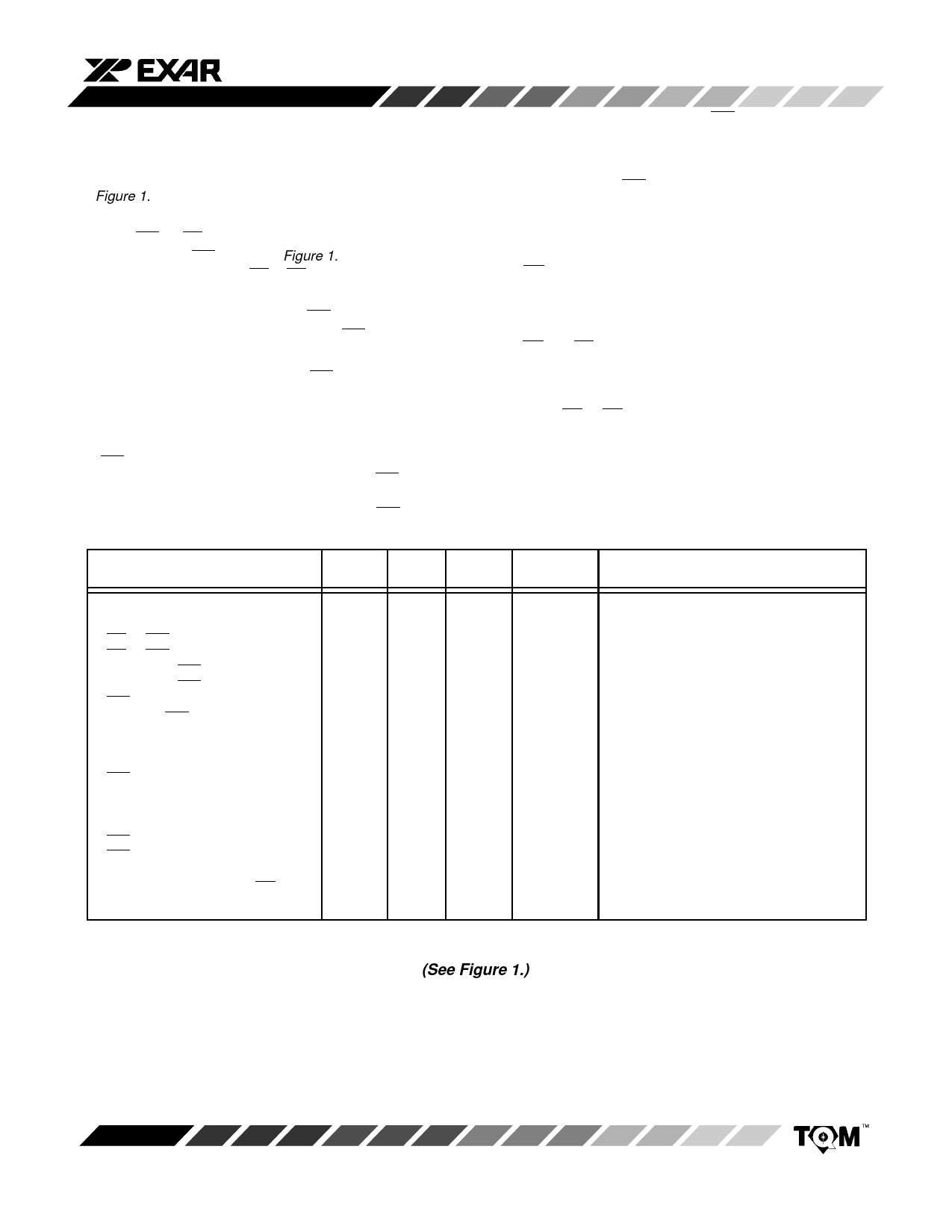
Figure 1. shows a complete timing diagram for the MP3274
convert start operation.
Either WR or CS may be used to initiate a conversion. We
recommend using WR as used in Figure 1. It is quieter and has
less propagation delay than CS. If CS is used to trigger the con-
version the specified set-up times will be longer.
A conversion is started by taking WR low, then high again
(conversion is enabled on the rising edge of WR). There are two
possible conditions that will affect conversion timing.
1. ADEN = 1. At the falling edge of WR, the input channel is
determined by the data present on the address bits. The
track and hold begins to settle after which STL returns low,
indicating that the multiplexer and the buffer amp have set-
tled to less than 1/2 LSB of final value. If the rising edge of
WR returns high prior to STL going low, conversion will begin
on the falling edge of STL. If the rising edge of WR is delayed
until after STL returns low, the input signal is sampled and
the conversion is started at the rising edge of WR giving the
user better control of the sampling time.
2. ADEN = 0. At the falling edge of WR the data present at the
address is ignored and the channel selected during the pre-
vious conversion remains selected. In this case the track
and hold settling time is omitted and STL never goes high. At
the rising edge of WR the input signal is sampled, and con-
version is started.
There are two possible states that the data outputs could be in
during a conversion.
1. If RD is held high during a conversion the outputs would re-
main high impedance throughout the conversion. This is the
preferred method of operation as any noise present on the
data bus is rejected.
2. If RD and CS are held low during a conversion, the data pre-
sent will be from the previous conversion until the present
conversion is completed when STS returns low. The data
from the new conversion will appear on the outputs. The
state of RD or CS should not change during a conversion.
Once a conversion is started and the STL or STS line goes
high, convert start commands will be ignored until the conver-
sion cycle is completed. The output data buffers cannot be en-
abled during conversion. In addition, all inputs and outputs
which change during conversion can introduce noise, and
should be avoided when possible.
ADC Write Timing
Time
Tmin to
Interval 25°C Tmax
Limits
Comments/Test Conditions
ADC Control Timing
CS to WR Set-Up Time
t1
CS to WR Hold Time
t2
Address to WR Set-Up Time
t3
Address to WR Hold Time
t4
WR Pulse Width
t5
ADEN to WR Set-Up Time
t6
ADC Conversion Timing
WR to STL Delay
t7
STL High (mux/amp settle)
t8
STL to STS Low (Converting)
t9
WR to STS High (ADEN = 0)
t12
WR to STS Low (ADEN = 1)
t10
STS High to Bus Relinquish Time
t13
STS Low to Data Valid (RD = 0)
t14
0
0
0
0
0
0
0
0
80
80
0
150 150
10
15
15
20
200 250
15
20
150 150
50
50
ns min
ns min
ns min
ns min
ns min
ns min
ns max
µs max
µs max
ns max
µs max
ns max
ns max
Load ckt of Figure 5, CL = 20 pF,
ADEN = 1
Load ckt of Figure 5, CL = 20 pF
Load ckt of Figure 5, CL = 20 pF
STL = 0 when ADEN = 0
Load ckt of Figure 4
Load ckt of Figure 3, CL = 20 pF
Table 2. ADC Write Timing
(See Figure 1.)
Rev. 4.00
7
Share Link: 