MP3274 데이터 시트보기 (PDF) - Exar Corporation
부품명
상세내역
일치하는 목록
MP3274 Datasheet PDF : 16 Pages
| |||
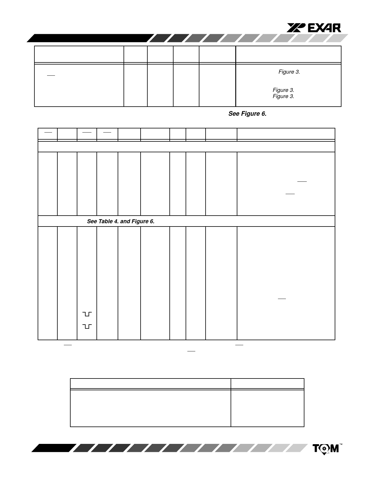
MP3274
Serial Data Output Timing
Time
Tmin to
Interval 25°C Tmax Limits
STS low to SDO (DB11) Valid,
RD = 0
Minimum clock high pulse width
SDC low to data valid delay
t20
50
50
t21
50
80
t22 150 ns 200
200 ns 250
ns max
ns max
ns max
ns max
Comments/Test Conditions
Load Ckt 4 of Figure 3.
Load ckt of Figure 3., CL = 20pF
Load ckt of Figure 3., CL = 100pF
Table 4. Serial Data Output Mode Timing (See Figure 6.)
CS PXS WR RD ADEN Data
ADC Channel Select and Start Convert
1
X
X
X
X
––
0
↓
X
1
X
Hi-Z
0
0
↓
1
0
Hi-Z
0
0
↓
1
1
Hi-Z
0
0
0
1
X
Hi-Z
0
0
↑
1
X
Hi-Z
0
0
1
1
X
Hi-Z
0
0
1
1
X
Hi-Z
Read ADC Data (See Table 4. and Figure 6.)
0
0
1
↓
X
––
STL STS DB0/SDC
0
0
X
0
0
X
0
0
X
↑
0
X
1
0
X
0
↑
X
↓
↑
X
0
↓
X
0
0
1
0
0
X
X
X MSB (DB11) 0
0
1
0
0
X
0
X
DB10 0
0
↓
0
0
X
0
X
DB10 0
0
0
0
0
X
0
X
DB10 0
0
↑
0
0
X
0
X
DB9
0
0
↓
0
0
X
↑
X
Hi-Z
0
0
X
0
X
1
X
X
Hi-Z
0
1
X
0
X
0
0
Hi-Z
0
↑
1
0
0
0
X MSB (DB11) 0
↓
1
Comments
No Operation
Serial mode enabled (1)
No operation if ADEN = 0
Input MUX channel selected, STL
set on falling edge of WR
MUX select disabled
Start convert on WR rising edge
Start convert on STL falling edge
STS goes low at end of conversion
Serial output (DB11/SDO) and
serial clock input (DB0/SDC)
enabled
MSB data available at DB11/SDO
Next significant bit shifted out to
DB11/SDO
No Operation
No Operation
Next significant bit shifted out to
DB11/SDO
Data outputs/SDC input disabled
Data outputs/RD disabled when
STS = 1
STL, MUX select disabled when
ADEN = 0
New data appears at DB11/SDO
on falling edge of STS
Note 1: If RD = 1, data outputs remain high impedance. It is recommended that RD will not change during a conver-
sion in order to reduce noise. It is further recommended that RD = 1 during conversion to reject any noise present on
the data bus.
Table 5. Logic Truth Table – Serial Data Output Mode
2’s Complement Output Code (Hexidecimal)
0111
0000
1111
1000
1111
0000
1111
0000
1110 (7fe) to 0111
0000 (000) to 0000
1111 (fff) to 0000
0000(800) to 1000
1111
0000
0000
0000
1111 (7ff)
0001 (001)
0000 (000)
0001 (801)
Ideal Transition Voltage
+FS – 1 1/2 LSB
0 V +1/2 LSB
0 V –1/2 LSB
–FS +1/2 LSB
Rev. 4.00
Table 6. Key Output Codes vs. Input Voltage (2’s Complement Code)
10
Share Link: 