MP3274 데이터 시트보기 (PDF) - Exar Corporation
부품명
상세내역
일치하는 목록
MP3274 Datasheet PDF : 16 Pages
| |||
MP3274
PRODUCT INFORMATION
Basic Description
The MP3274 is a fault protected data acquisition subsystem
available in monolithic form. This product contains all of the cir-
cuitry necessary to acquire 32 channels of differential or single-
ended analog signals at 10 V input range and 15kHz
bandwidth. Connections to power, the analog input signals and
the digital system are all that is required. The MP3274’s input
circuitry is protected against active input signals present with the
MP3274 power off. This is also the case for any channel exceed-
TIMING
ing the MP3274 analog input dynamic range without interfering
with the channel being digitized. The channel address and
channel conversion can be managed in two ways: random
channel conversion or same channel conversion. Circuitry on
the chip adds a MUX/instrumentation amp settling delay, when a
new channel is selected (ADEN = 1). Conversion start is initi-
ated without delay for the single-channel case (ADEN = 0). Data
is available in either parallel or serial format.
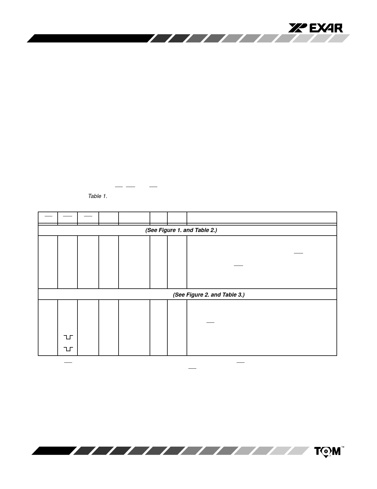
Control and Timing Considerations – Parallel Mode (PXS = 1)
The MP3274 can be operated in the stand-alone mode, with
one line for control and everything else hard-wired; or under mi-
croprocessor control, where changes can be made dynamically.
There are 4 control lines: ADEN, CS, WR, and RD with their
functions described in Table 1.
PXS is the control pin for formatting data for serial or parallel
control.
CS WR RD ADEN Data STL STS
Comments
ADC Channel Select and Start Convert (See Figure 1. and Table 2.)
1
X
X
X
––
0
0 No operation
0
↓
1
0
Hi-Z
0
0 No operation if ADEN = 0
0
↓
1
1
Hi-Z
↑
0 Input MUX channel selected, STL set on WR falling edge
0
0
1
X
Hi-Z
1
0 MUX select disabled
0
↑
1
X
Hi-Z
0
↑ Start convert on WR rising edge
0
1
1
X
Hi-Z
↓
↑ Start convert on STL falling edge
0
1
1
X
Hi-Z
0
↓ STS goes low at end of conversion
Read ADC Data – Parallel Output Mode (PXS = 1) (See Figure 2. and Table 3.)
0
1
↓
X
––
0
0 Data outputs enabled
0
X
0
X
ADC
0
0 Data from previous conversion on data bus
0
X
↑
X
Hi-Z
0
0 Data outputs disabled
0
1
X
X
Hi-Z
0
1 Data/RD disabled while STS high
0
X
0
X Last ADC 1
0 Data from last conversion on data bus
0
0
0
Hi-Z
0
↑ STL, MUX select disabled with ADEN = 0,
data outputs disabled on STS rising edge
0
0
X
ADC
0
↓ New data appears on data bus on falling edge of STS
Note 1: If RD = 1, data outputs remain high impedance. It is recommended that RD will not change during a conver-
sion in order to reduce noise. It is further recommended that RD = 1 during conversion to reject any noise present on
the data bus.
Table 1. Logic Truth Table for PXS = 1 (Parallel Mode)
Rev. 4.00
6
Share Link: 