LT5524 데이터 시트보기 (PDF) - Linear Technology
부품명
상세내역
일치하는 목록
LT5524 Datasheet PDF : 16 Pages
| |||
LT5524
PI FU CTIO S
EN (Pin 1): Enable Pin for Amplifier. When the input
voltage is higher than 3V, the amplifier is turned on. When
the input voltage is less than or equal to 0.6V, the amplifier
is turned off. This pin is internally pulled to ground if not
connected.
VCC1 (Pin 2): Power Supply. This pin is internally connected
to VCC2 (Pin 19). Decoupling capacitors (1000pF and 0.1µF
for example) may be required in some applications.
GND (Pins 3, 4, 7, 8, 13, 14, 17, 18): Ground.
IN+ (Pin 5): Positive Signal Input Pin with Internal DC
Bias.
IN– (Pin 6): Negative Signal Input Pin with Internal DC
Bias.
PGA0 (Pin 9): Amplifier PGA Control Input Pin for the 1.5dB
Attenuation Step (see Programmable Gain table). Input is
high when the input voltage is greater than 3V. Input is low
when the input voltage is less than or equal to 0.6V. This
pin is internally pulled to ground if not connected.
PGA1 (Pin 10): Amplifier PGA Control Input Pin for the 3dB
Attenuation Step (see Programmable Gain table). Input is
high when the input voltage is greater than 3V. Input is low
when the input voltage is less than or equal to 0.6V. This
pin is internally pulled to ground if not connected.
PGA2 (Pin 11): Amplifier PGA Control Input Pin for the 6dB
Attenuation Step (see Programmable Gain table). Input is
high when the input voltage is greater than 3V. Input is low
when the input voltage is less than or equal to 0.6V. This
pin is internally pulled to ground if not connected.
PGA3 (Pin 12): Amplifier PGA Control Input Pin for 12dB
Attenuation Step (see Programmable Gain table). Input is
high when the input voltage is greater than 3V. Input is low
when the input voltage is less than or equal to 0.6V. This
pin is internally pulled to ground if not connected.
OUT+ (Pin 15): Positive Amplifier Output. A transformer
with center tap tied to VCC or a choke inductor is recom-
mended to source the DC quiescent current.
OUT– (Pin 16): Negative Amplifier Output. A transformer
with center tap tied to VCC or a choke inductor is recom-
mended to source the DC quiescent current.
VCC2 (Pin 19): Power Supply. This pin is internally con-
nected to VCC1 (Pin 2).
NC (Pin 20): Not Connected.
Exposed Pad (Pin 21): Ground. This pin must be soldered
to the printed circuit board ground plane for good heat
transfer.
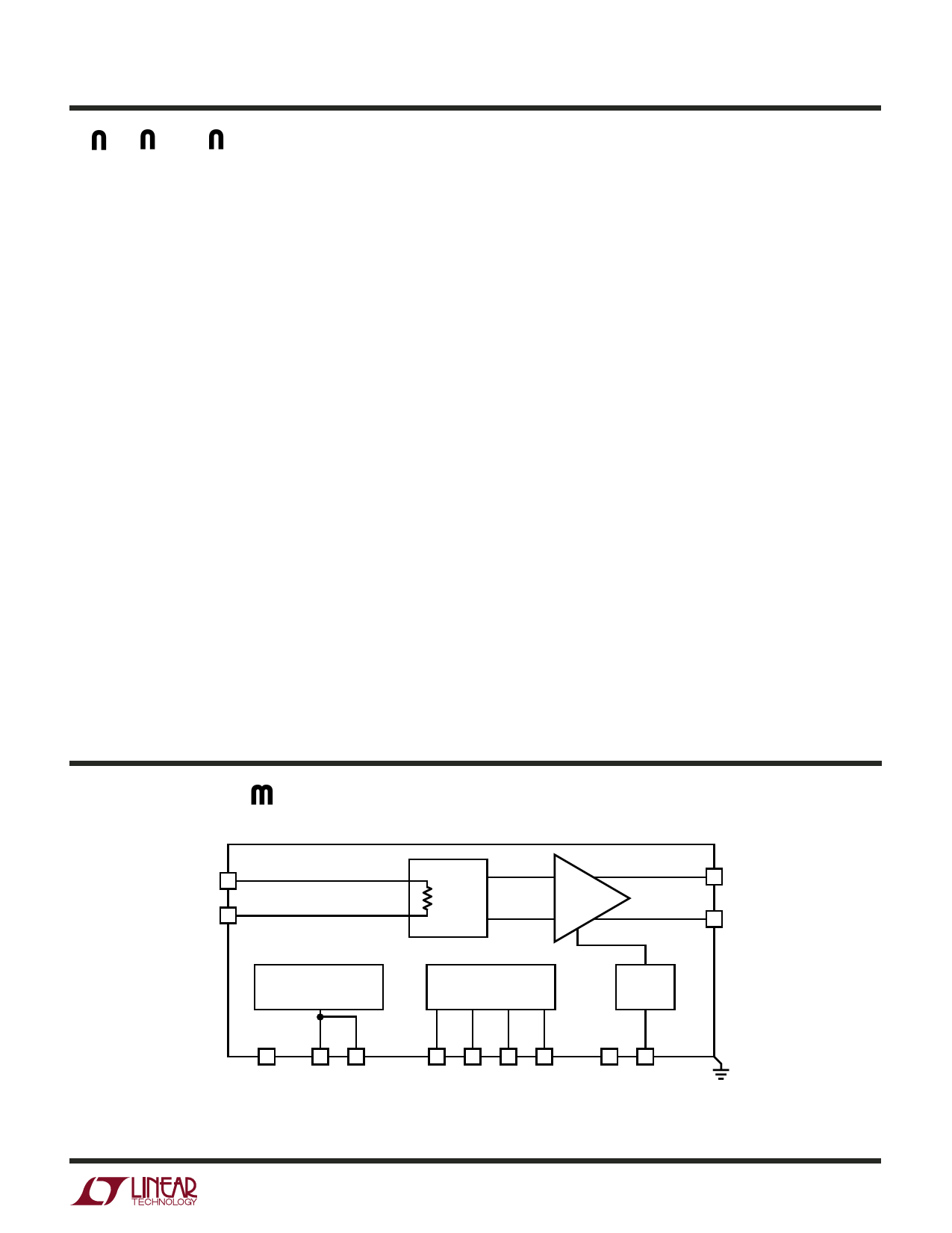
BLOCK DIAGRA
LT5524
IN+
5
6 IN–
ATTENUATOR
RIN
100Ω
AMPLIFIER
OUT–
16
OUT+
15
VOLTAGE REGULATOR
AND BIAS
GAIN CONTROL
LOGIC
ENABLE
CONTROL
GND (3, 4, 7, 8
13, 14, 17, 18)
VCC1 VCC2
2 19
PGA3 PGA2 PGA1 PGA0
12 11 10 9
Figure 1. Functional Block Diagram
NC EN
20 1
21
5524 F01
5524f
7
Share Link: 