LT5524 데이터 시트보기 (PDF) - Linear Technology
부품명
상세내역
일치하는 목록
LT5524 Datasheet PDF : 16 Pages
| |||
LT5524
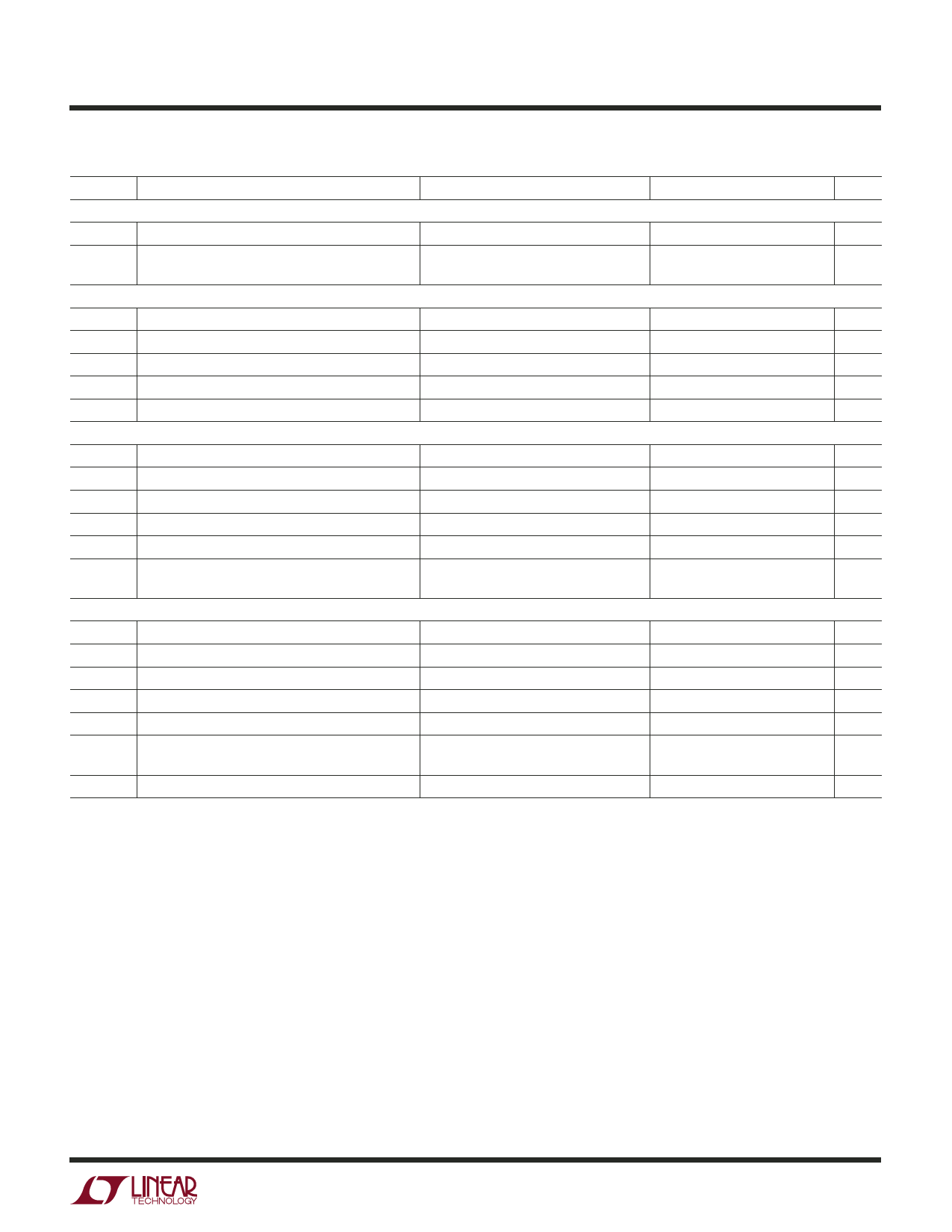
DC ELECTRICAL CHARACTERISTICS VCC = 5V, VCCO = 5V, EN = 3V, TA = 25°C, unless otherwise noted.
(Note 7) (Test circuits shown in Figures 9 and 10)
SYMBOL PARAMETER
CONDITIONS
MIN
TYP
MAX UNITS
Normal Operating Conditions
VCC
Supply Voltage (Pins 2, 19)
(Note 4)
4.75
5
5.25
V
VCCO
OUT+, OUT– Output Pin DC Common Mode Voltage OUT+, OUT– Connected to VOSUP via
3
5
5.5
V
Choke Inductors or Resistors (Note 5)
Shutdown DC Characteristics, EN = 0.6V
VIN(BIAS) IN+, IN– Bias Voltage
IIL(PGA)
PGAO, PGA1, PGA2, PGA3 Input Current
IIH(PGA)
IOUT
PGAO, PGA1, PGA2, PGA3 Input Current
OUT+, OUT– Current
ICC
VCC Supply Current
Enable and PGA Inputs DC Characteristics
Max Gain (Note 6)
VIN = 0.6V
VIN = 5V
All Gain Settings
All Gain Settings (Note 4)
1.15
1.3
1.5
V
20
µA
20
µA
20
µA
44
100
µA
VIL
VIH
IIL(PGA)
IIH(PGA)
IIL(EN)
IIH(EN)
EN and PGAx Input Low Voltage
EN and PGAx Input High Voltage
PGAO, PGA1, PGA2, PGA3 Input Current
PGAO, PGA1, PGA2, PGA3 Input Current
EN Input Current
EN Input Current
DC Characteristics, EN = 3V
VIN(BIAS) IN+, IN– Bias Voltage
RIN
Input Differential Resistance
gm
Amplifier Transconductance
IOUT
OUT+, OUT– Quiescent Current
IOUT(OFFSET) Output Current Mismatch
ICC
VCC1 + VCC2 Supply Current
x = 0, 1, 2, 3
x = 0, 1, 2, 3
VIN = 0.6V
VIN = 3V and 5V
VIN = 0.6V
VIN = 3V
VIN = 5V
Max Gain (Note 6)
All Gain Settings (DC)
Max Gain
All Gain Settings, VOUT = 5V
All Gain Settings, IN+, IN– Open
Max Gain (Note 4)
Min Gain (Note 4)
0.6
V
3
V
20
µA
15
30
µA
4
20
µA
18
µA
38
100
µA
1.34
1.48
1.65
V
122
Ω
0.15
S
17
20
24
mA
100
µA
34
40
mA
36
43
mA
ICC(TOTAL) Total Supply Current
ICC + 2 • IOUT (Max Gain)
75
91
mA
5524f
3
Share Link: 