GF9105A 데이터 시트보기 (PDF) - Unspecified
부품명
상세내역
일치하는 목록
GF9105A Datasheet PDF : 37 Pages
| |||
There are seven basic blocks that make up the GF9105A. These are:
• Input De-multiplexer
• Horizontal Blanking and Input Offset Adjustment
• FIR Filters
• 3x3 Color Space Converter and KEY Scaler
• Output Offset Adjustment
• Output Clipping
• Output Multiplexer
Since the GF9105A Processing Core functionality depends on the state of INT/DEC, device operation will be described first
for the case where INT/DEC is set high and then for the case where INT/DEC is set low.
GF9105A OPERATION IN INTERPOLATION MODE (INT/DEC = 1)
Refer to Figures 5a and 5c for a functional block diagram of GF9105A operation with INT/DEC = 1
BIT WEIGHTING
Although the input data ports are physically 13 bits or 11 bits wide, the GF9105A Processing Core is limited to processing
10 or 8-bit unsigned input data while INT/DEC is set high. It should be noted that while INT/DEC is set low, the GF9105A
Processing Core will accept up to 13 bit input data. Refer to later sections for a description of Processing Core functionality
while INT/DEC is set low.
As mentioned above, the GF9105A is limited to processing 10 or 8-bit unsigned input data while INT/DEC is set high. This
input data must be properly embedded within the input data ports. The following table illustrates how to properly embed 10
or 8-bit data within the 13 bit data ports. Note that when OUTPUT/INPUT=0 and HVF_OUT=1, P112, P212 and P312 (which
corresponds to b12) are outputs rather than inputs. These 3 outputs are used for presenting output H, V and F output signals.
The user should be careful to ensure that P112, P212 and P312,are not driven by upstream logic when OUTPUT/INPUT=0 and
HVF_OUT=1. Other unused inputs should be set low by the user.
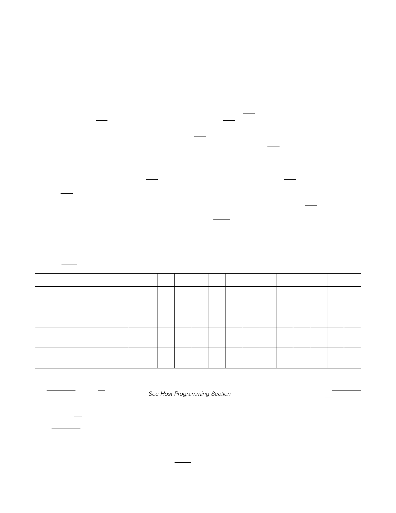
OUTPUT/INPUT = 0, HVF_OUT = 0
DATA PORT REFERENCE
Input Port: P112..0 to P312..0
Embedded 10 bit signal
Input Port: P410..0
Embedded 10 bit signal
Input Port: P112..0 to P312..0
Embedded 8 bit signal
Input Port: P410..0
Embedded 8 bit signal
13 BIT PHYSICAL INTERFACE
b12
b11 b10 b9
b8
b7
b6
b5
b4
b3
b2
b1
b0
0
0
0
b9
b8
b7
b6
b5
b4
b3
b2
b1
b0
NA
NA
0
b9
b8
b7
b6
b5
b4
b3
b2
b1
b0
0
0
0
b7
b6
b5
b4
b3
b2
b1
b0
0
0
NA
NA
0
b7
b6
b5
b4
b3
b2
b1
b0
0
0
INPUT DE-MULTIPLEXER
The MUXED_IN and SL/DL_IN control bits (See Host Programming Section) determine the input data format. The MUXED_IN
control bit is used to identify whether the incoming data is in a multiplexed or non-multiplexed format. The SL/DL_IN control
bit is used to identify whether the incoming data is in a single link or dual link format.
Dual Link (SL/DL_IN = 0)
While MUXED_IN is set low, input data is assumed to be two 10 bit streams in 4:2:2:4 or 4:4:4:4 data format as shown in
Figure 7a. The input de-multiplexer separates the 4:2:2:4 or 4:4:4:4 input signals into four channels of Y/G, CB/B, CR/R and
KEY data. These four data streams are then passed to the next processing section.
When operating with multiplexed 4:2:2:4 or 4:4:4:4 input data, the 4:2:2 data stream enters the GF9105A Processing Core
from Processing Core input port C1. While OUTPUT/INPUT=0 Processing Core port C1 corresponds to device data port P1
521 - 88 - 03
10
Share Link: 