AN-136 데이터 시트보기 (PDF) - Integrated Device Technology
부품명
상세내역
일치하는 목록
AN-136 Datasheet PDF : 12 Pages
| |||
A NEW GENERATION OF TAG SRAMS—THE IDT71215 AND IDT71216
APPLICATION NOTE AN-136
will ripple through to BRDY/TA), or if data SRAM accesses
require wait states (it’s necessary to toggle BRDY/TA from
cycle to cycle). For those times when neither device is driving
BRDY/TA, a pull-up resistor is used to keep the signal high. In
this case, it’s suggested that the controller drive BRDY/TA
high before putting it in a high impedance state. Thus, the
resistor is never used to generate a low to high transition and
therefore can be weak (3 KΩ to 20 KΩ). Also, both the 71215/
16 and controller can remain off the BRDY/TA bus for ex-
tended periods of time if so desired. With this approach,
BRDYIN or TAIN (Burst Ready Input, Transfer Acknowledge
Input) is tied high.
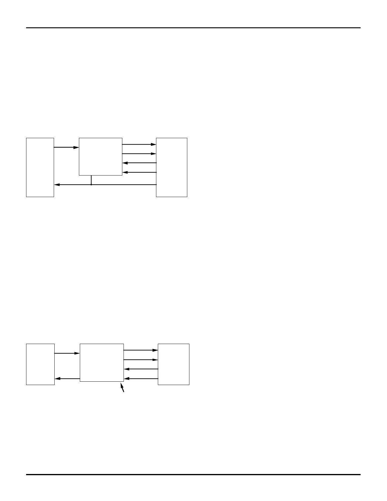
66MHz
PENTIUM
A(5:30)
71215 TAG
CHIP SET
A(0:13)
TAG(0:11)
MATCH
STATUS BITS
BRDYH
BRDY BRDYOE
BRDYH
BRDYOE
BRDY
BRDY
The BRDY sources are totem-pole, NOT open-drain
3176 drw 09
Figure 9. Combining BRDY/TA : Bussing Option
REDUCED POWER
For the increasing number of applications that require a low
power standby mode, the 71215/16 includes an asynchro-
nous power down pin (PWRDN). When it is driven low, both
the tag and status memories are shut down to save consider-
ably on power consumption. For optimum power savings, all
input and bidirectional signals should also be held at CMOS
voltage levels (near VCC or VSS). During power down, all
outputs are placed in a high impedance state and all data is
retained. All writes should be allowed to complete before
PWRDN is asserted. There is no minimum time that it must be
low. When exiting the power down state, there is only a very
short delay after the rising edge of PWRDN before normal
activity can be resumed.
SYSTEM USAGE
For applications not using the entire 12-bit tag field, the
unused TAG I/O pins should be pulled either high or low
through 1 KΩ to 5 KΩ resistors. For applications not using the
entire 3-bit status field, the unused inputs may be tied directly
to VCC or VSS, and the unused outputs are left unconnected.
All other unused inputs should be tied either to VCC or VSS as
appropriate for their function. This includes unused address
signals ift only part of the depth of the 71215/16 is used.
The second approach is to have the cache/memory con-
troller drive it’s BRDY/TA output into the BRDYIN/TAIN input
on the 71215/16 at all times. Inside the 71215/16, BRDYIN/
TAIN is registered by the clock then ANDed (negative logic
ORed) with the internally generated BRDY/TA. For this
approach, BRDYOE/TAOE is tied permanently low. The
controller no longer generates BRDYOE/TAOE, but instead
must generate BRDY/TA one cycle earlier because it is
delayed by one cycle in reaching the CPU. Note that BRDYH/
TAH only enables or disables the BRDY/TA generated inside
the 71215/16, and does not affect the propagation of BRDYIN/
TAIN through to the BRDY/TA output. Figure 10 shows this
approach for the 71215 and Pentium.
66MHz
PENTIUM
A(5:30)
71215 TAG
A(0:13)
TAG(0:11)
CHIP SET
MATCH
STATUS BITS
BRDY
BRDYH
BRDY BRDYIN
BRDYH
BRDY
BRDYIN is registered 3176 drw 10
Figure 10. Combining BRDY/TA : Pass-Through Option
BRDY/TA functions similar to MATCH (but opposite in
polarity) when the 71215/16 is not in match mode. It is high
impedance when the chip is deselected (or BRDYOE/TAOE is
high), and otherwise is driven high when out of match mode.
8
Share Link: 