MK5027(2003) 데이터 시트보기 (PDF) - STMicroelectronics
부품명
상세내역
일치하는 목록
MK5027 Datasheet PDF : 19 Pages
| |||
MK5027
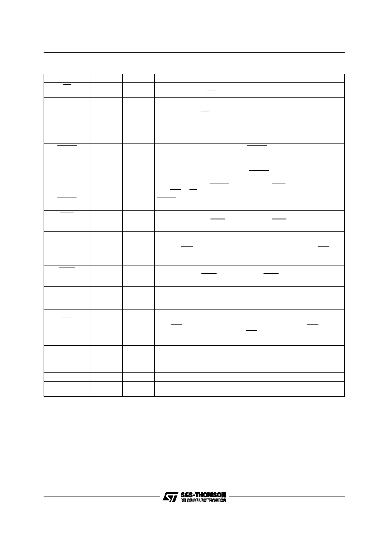
Table 1: Pin Description (continued)
Signal Name
CS
ADR
Pin(s)
20
21
Type
I
I
Descriplion
CHIP SELECT indicates, when low, that the MK5027 is the slave device
for the data transfer.CS must be valid througout the enture transaction.
ADDRESS selects the Register Address Port or the Register Data Port. It
must be valid throughout the data portion of the transfer and is only used
by the chip when CS is low.
READY
RESET
TCLK
DTR
RTS
RCLK
SYSCLK
TD
DSR
CTS
RD
A<23:16>
VSS-GND
VCC
22
23
25
26
27
28
29
30
31
32-39
1, 24
48
IO/OD
I
I
IO
I
I
O
IO
I
O/3S
ADR
LOW
HIGH
PORT
REGISTER DATA PORT
REGISTER ADDRESS PORT
When the MK5027 is a Bus Master, READY is an asynchronous
acknowledgement from the bus memory that memory will accept data in a
WRITE cycle or that memory has put data on the DAL lines in a READ
cycle.
As a bus Slave, the MK5027 asserts READY when it has put data on the
DAL lines during a READ cycle or is about to take data from the DAL lines
during WRITE cycle. READY is a response to DAS and it will be released
after DAS or CS is negated.
RESET is the Bus signal that will cause MK5027 to cease operation, clear
its internal logic and enter an idle state with the Power Off bit of CSR0 set.
TRANSMIT CLOCK. A 1x clock input for transmitter timing. TD changes
on the falling edge of TCLK. The frequency of TCLK may not be greater
than the frequency of SYSCLK.
DATA TERMINAL READY, REQUEST TO SEND. Modem control pin. Pin
26 is configurable through CSR5. This pin can be programmed to behave
as output RTS or as programmable IO pin DTR. If configured as RTS, the
MK5027 will assert this pin if it has data to send and throughout the
transmission of a signal unit.
RECEIVE CLOCK. A 1x clock input for receiver timing. RD is sampled on
the rising edge of RCLK. The frequency of RCLK may not be greater than
the frequency of SYSCLK.
SYSTEM CLOCK. System clock used for internal timing of the MK5027.
SYSCLK should be a square wave, of frequency up to 10MHz.
TRANSMIT DATA. Transmit serial data output.
DATA SET READY, CLEAR TO SEND. Modem Control Pin. Pin 30 is
configurable through CSR5. This pin can be programmed to behave as
input CTS or as programmable IO pin DSR. If configured as CTS, the
MK5027 will transmit all ones while CTS is high.
RECEIVE DATA. Received serial data input.
Address bits <23:16> used in conjunction with DAL <15:00> to produce a
24 bit address. MK5027 drives these lines only as a Bus Master.
A23-A20 may be driven continuously as described in the CSR4<7> BAEN
bit.
Ground Pins
Power Supply Pin
+5.0 VDC ± 5%
4/19
Share Link: 