MK5027(2003) 데이터 시트보기 (PDF) - STMicroelectronics
부품명
상세내역
일치하는 목록
MK5027 Datasheet PDF : 19 Pages
| |||
MK5027
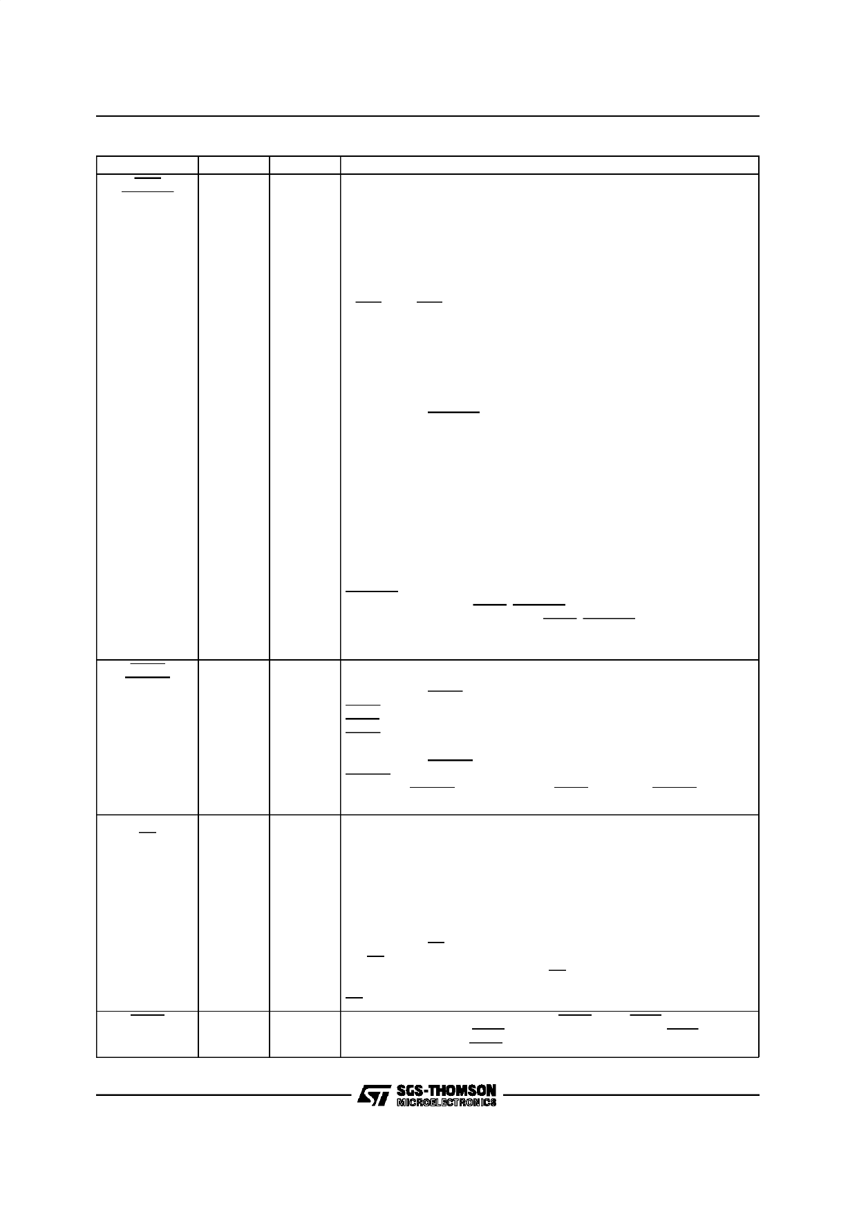
Table 1: Pin Description (continued)
Signal Name
BM1
BUSAKO
Pin(s)
16
Type
O/3S
Descriplion
Pins 15 and 16 are programmable though bit 00 of CSR4 (BCON).
If CSR4<00> BCON = 0,
I/O PIN 15 = BMO (O/3S)
I/O PIN 16 = BM1 (O/3S)
BYTE MASK<1:0> indicates the byte(s) on the DAL to be read or written
during this bus transaction. MK5027 drives these lines only as a Bus
Master. MK5027 ignores the BM lines when it is a Bus Slave.
Byte selection is done as outlined in the following table.
BM1
BM0
TYPE OF TRANSFER
LOW
LOW
ENTIRE WORD
LOW
HIGH
UPPER BYTE (DAL<15:08>)
HIGH LOW
LOWER BYTE (DAL<07:00>)
HIGH HIGH
NONE
If CSR4<00>BCON = 1,
I/O PIN 15 = BYTE (O/3S)
I/O PIN 16 = BUSAKO (O)
Byte selection is done using the BYTE line and DAL<00> latched during
the address portion of the bus transaction. MK5027 drives BYTE only a
Bus Master and ignores it when a Bus Slave. Byte selection is done as
outlined in the following table.
BYTE DAL<00> TYPE OF TRANSFER
LOW
LOW
HIGH
HIGH
LOW
HIGH
LOW
HIGH
ENTIRE WORD
ILLEGAL CONDITION
LOWER BYTE
UPPER BYTE
HOLD
BUSRQ
ALE
AS
HLDA
BUSAKO is a bus request daisy chain output. If MK5027 is not requesting
the bus and it receives HLDA, BUSAKO will be driven low. If MK5027 is
requesting the bus when it receives HLDA, BUSAKO will remain high.
Note: All transfers are entire word unless the MK5027 is configured for 8
bit operation.
17
IO/OD Pins 17 is configured through bit 0 of CSR4.
If CSR4<00> BCON = 0,
I/O PIN 17 = HOLD
HOLD request is asserted by MK5027 when it requires a DMA cycle, if
HLDA is inactive, regardless of the previous state of the HOLD pin.
HOLD is held low for the entire ensuing bus transaction.
If CSR4<00> BCON = 1,
I/O PIN 17 = BUSRQ
BUSRQ is asserted by MK5027 when it requires a DMA cycle if the prior
state of the BUSRQ pin was high and HLDA is inactive. BUSRQ is held
low for the entire ensuing bus transaction.
18
O/3S The active level of ADDRESS STROBE is programmable through CSR4.
The address portion of a bus transfer occurs while this signal is at its
asserted level. This signal is driven by MK5027 while it is the BUS
MASTER. At all other times, the signal is tristated.
If CSR4<01> ACON = 0,
I/O PIN 18 = ALE
ADDRESS LATCH ENABLE is used to demultiplex the DAL lines and define
the address portion of the transfer and remains low during the data portion.
If CSR4<01> ACON = 1,
I/O PIN 18 = AS
As AS, the signal pulses low during the address portion of the bus
transfer. The low to high transition of AS can be used by a slave device to
strobe the address into a register.
AS is effectively the inversion of ALE.
19
I
HOLD AKNOWLEDGE is the response to HOLD. When HLDA is low in response
to MK5027’s assertion of HOLD, the MK5027 is the Bus Master. HLDA should be
desasserted ONLY after HOLD has been released by the MK5027.
3/19
Share Link: 