CS5111 데이터 시트보기 (PDF) - Cherry semiconductor
부품명
상세내역
일치하는 목록
CS5111
Cherry semiconductor

CS5111 Datasheet PDF : 10 Pages
| |||
Circuit Description: continued
VIN
VLIN
IBIAS
RBIAS
64.9kΩ
COSC
Oscillator
VREG
Over Voltage
COMP
COMP
Logic
Base Drive
VSW
1.4A
VOUT
COUT
Current Sense Amplifier
-
RS
Gnd
ENABLE
-
Switcher Shutdown
1.25V
Bandgap
Reference
Switcher
R1
VFB1
Error
Amplifier -
Multiplexer
VFB2
R2
R3
SELECT
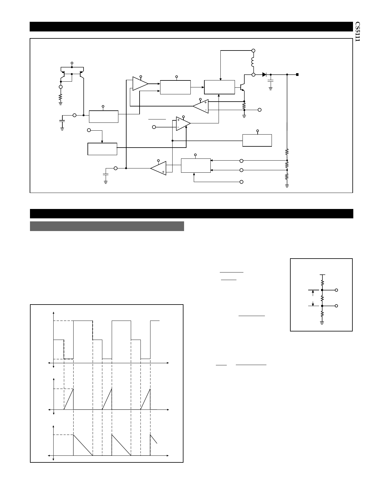
Figure 6: Block diagram of the 1.4A current mode control switching regulator portion of the CS5111 in a boost configuration.
Application Notes
Design Procedure for Boost Topology
This section outlines a procedure for designing a boost switch-
ing power supply operating in the discontinuous mode.
Step 1
Determine the output power required by the load.
POUT = IOUTVOUT
(1)
Step 2
Choose COSC based on the target oscillator frequency with an
external resistor value, RBIAS = 64.9kΩ. (See Figure 1d).
VSW
VOUT
Step 3
Next select the output voltage feedback sense resistor
divider as follows (Figure 8).
For VFB1 active, choose a value for R1 and then solve for
REQ where:
REQ =
R1 .
VOUT
VFB1
-1
(3a)
For VFB2 active, find:
( ) VFB1 = VOUT
REQ
R1 + REQ
, (3b)
VOUT
{ VR2
REQ
R1
VFB1
R2
VFB2
R3
VIN
VSAT
0
ISW
IPeak
and then calculate R2 where:
Figure 8. Feedback sense
resistor divider connected
between VOUT and ground.
t
R2 =
VR2
IR2
=
VFB1 - VFB2
VFB1/REQ
. (3c)
Then find R3, where:
0
ID
IPeak
t
R3 = REQ - R2.
(3d)
0
t
Figure 7: Voltage and current waveforms for boost topology in CS5111.
7
Share Link: