CS5111 데이터 시트보기 (PDF) - Cherry semiconductor
부품명
상세내역
일치하는 목록
CS5111
Cherry semiconductor

CS5111 Datasheet PDF : 10 Pages
| |||
Circuit Description: continued
If a correct watchdog signal is not received within the
specified time a reset pulse train is issued until the correct
watchdog signal is received. The nominal reset signal in
this case is a 5 volt square wave with a 50% duty cycle as
shown in Figure 4.
The RESET signal frequency is given by:
fRESET =
1
2(tWDI)
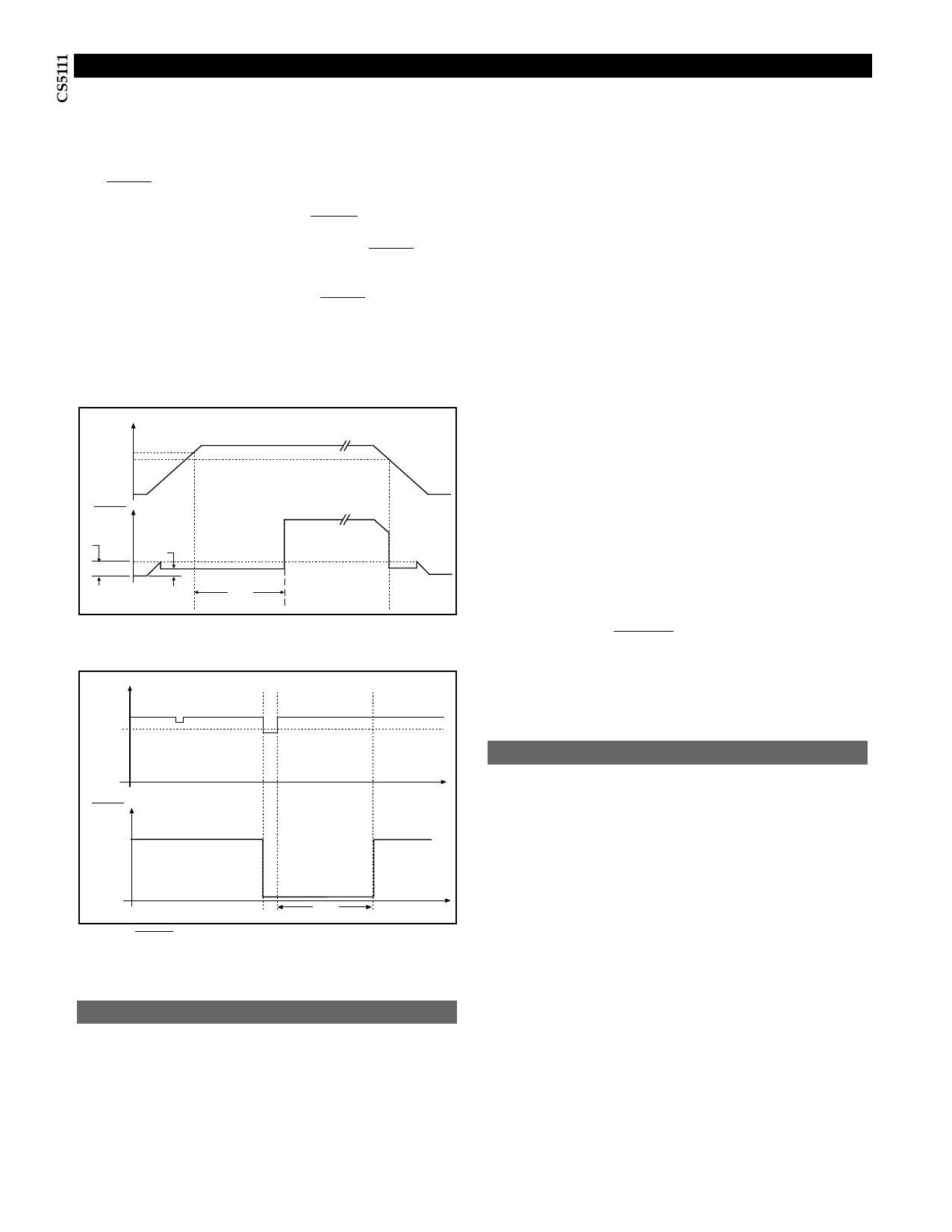
The Power On Reset (POR) and low voltage RESET use
the same circuitry and issue a reset when the linear output
voltage is below the regulation limit. After VLIN rises
above the minimum specified value, RESET remains low
for a fixed period tPOR as shown in Figure 5.
The POR delay (tPOR) is given by:
tPOR = 1.353 × CDelay RBIAS
VLIN
4.45V
4.25V
RESET
VRPEAK
VRLO
tPOR
Figure 5a. The power on reset time interval (tPOR) begins when VLIN
rises above 4.45V (typical).
VLIN
5V
4.25V
RESET
5V
tPOR
Figure 5b. RESET signal is issued whenever VLIN falls below 4.25V
(typical).
Current Mode PWM Switching Circuitry
The current mode PWM switching voltage regulator con-
tains an error amplifier with selectable feedback inputs, a
current sense amplifier, an adjustable oscillator and a 1.4A
output power switch with antisaturation control. The
switching regulator and external components, connected
in a boost configuration, are shown in Figure 6.
The switching regulator begins operation when VREG and
VIN are raised above 5 volts. VREG is required since the
switching supply’s control circuitry is powered through
VLIN. VIN supplies the base drive to the switcher output
transistor.
The output transistor turns on when the oscillator starts to
charge the capacitor on COSC. The output current will
develop a voltage drop across the internal sense resistor
(RS). This voltage drop produces a proportional voltage at
the output of the current sense amplifier, which is com-
pared to the output of the error amplifier. The error ampli-
fier generates an output voltage which is proportional to
the difference between the scaled down output boost volt-
age (VFB1 or VFB2) and the internal bandgap voltage refer-
ence. Once the current sense amplifier output exceeds the
error amplifier’s output voltage, the output transistor is
turned off.
The energy stored in the inductor during the output tran-
sistor on time is transferred to the load when the output
transistor is turned off. The output transistor is turned
back on at the next rising edge of the oscillator. On a cycle
by cycle basis, the current mode controller in a discontinu-
ous mode of operation charges the inductor to the appro-
priate amount of energy, based on the energy demand of
the load. Figure 7 shows the typical current and voltage
waveforms for a boost supply operating in the discontinu-
ous mode.
NOTES:
1. Refer to Figure 1d to determine oscillator frequency.
2. The switching regulator can be disabled by providing a
logic high at the ENABLE input.
3. The boost output voltage can be controlled dynamically
by the feedback select input. If select is open, VFB2 is
selected. If select is low, then VFB1 is selected.
Protection Circuitry
If the input voltage at VREG is increased above the over-
voltage threshold, the drive to the linear and switcher out-
put transistors is shut off. Therefore, VLIN is disabled and
VSW can not be pulled low.
The current out of VLIN is sensed in order to limit exces-
sive power dissipation in the linear output transistor over
the output range of 0V to regulation. Also, the current into
VSW is sensed in order to provide the current limit func-
tion in the switcher output transistor.
If the die temperature is increased above 160°C, either due
to excessive ambient temperature or excessive power dis-
sipation, the drive to the linear output transistor is
reduced proportionally with increasing die temperature.
Therefore, VLIN will decrease with increasing die tempera-
ture above 160°C. Since the switcher control circuitry is
powered through VLIN, the switcher performance, includ-
ing current limit, will be affected by the decrease in VLIN.
6
Share Link: