CS5111 데이터 시트보기 (PDF) - Cherry semiconductor
부품명
상세내역
일치하는 목록
CS5111
Cherry semiconductor

CS5111 Datasheet PDF : 10 Pages
| |||
VREG
Over Voltage
1.25V
IBIAS
RBIAS
64.9kΩ
Cdelay
WDI
Bandgap
Reference
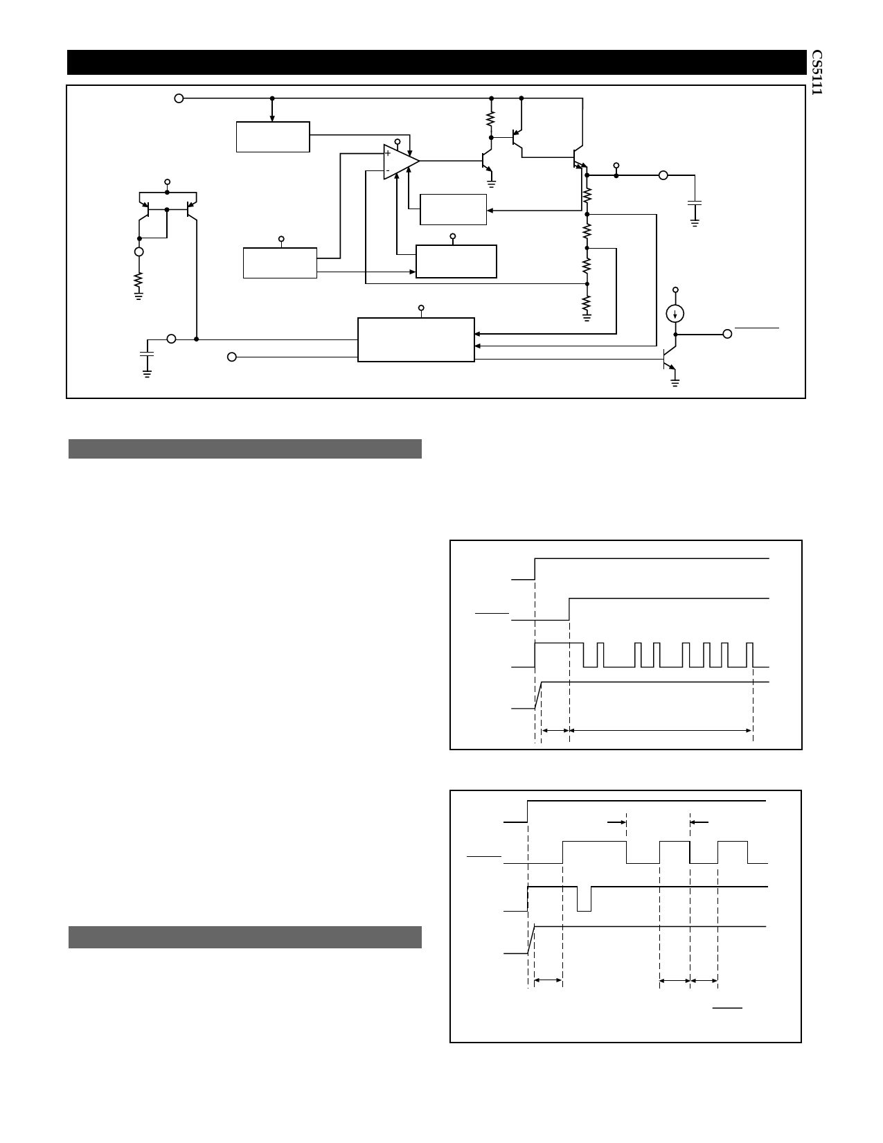
Circuit Description
R1
Linear
Error
Q2
-
Amplifier Q1
Current
Limit
Over
Temperature
RESET &
Watchdog Timer
Q3
R2
R3
R4
R5
VLIN
COUT = 100µF
ESR < 8Ω
RESET
Figure 2. Block diagram of 5V linear regulator portion of the CS5111.
5V Linear Regulator
The 5V linear regulator consists of an error amplifier,
bandgap voltage reference, and a composite pass transistor.
The 5V linear regulator circuitry is shown in Figure 2.
When an unregulated voltage greater than 6.6V is applied
to the VREG input, a 5V regulated DC voltage will be pre-
sent at VLIN. For proper operation of the 5V linear regula-
tor, the IBIAS lead must have a 64.9kΩ pull down resistor to
ground. A 100µF or larger capacitor with an ESR <8Ω
must be connected between VLIN and ground. To operate
the 5V linear regulator as an independent regulator (i.e.
separate from the switching supply), the input voltage
must be tied to the VREG lead.
As the voltage at the VREG input is increased, Q1 is turned
on. Q1 provides base drive for Q2 which in turn provides
base current for Q3. As Q3 is turned on, the output voltage,
VLIN, begins to rise as Q3’s output current charges the out-
put capacitor, COUT. Once VLIN rises to a certain level, the
error amplifier becomes biased and provides the appropri-
ate amount of base current to Q1. The error amplifier mon-
itors the scaled output voltage via an internal voltage
divider, R2 through R5, and compares it to the bandgap
voltage reference. The error amplifier output or error sig-
nal is an output current equal to the error amplifier’s input
differential voltage times the transconductance of the
amplifier. Therefore, the error amplifier varies the base
current to Q1, which provides bias to Q2 and Q3, based on
the difference between the reference voltage and the
scaled VLIN output voltage.
Using CDelay = 0.1µF and RBIAS = 64.9kΩ gives a time rang-
ing from 6.25ms to 11ms assuming ideal components. Based
on this, the software must be written so that the watchdog
arrives at least every 6.25ms. In practice, the tolerance of
CDelay and RBIAS must be taken into account when calculat-
ing the minimum watchdog time (tWDI).
VREG
RESET
WDI
VLIN
tPOR
Normal Operation
Figure 3. Timing diagram for normal regulator operation.
VREG
RESET
WDI
50% Duty
Cycle
Control Functions
The watchdog timer circuitry monitors an input signal
(WDI) from the microprocessor. It responds to the falling
edge of this watchdog signal which it expects to see within
an externally programmable time (see Figure 3).
The watchdog time is given by:
tWDI = 1.353 × CDelay RBIAS
VLIN
tPOR
AB
A: Watchdog waiting for B: RESET stays low for
low-going transition on tWDI time.
WDI
Figure 4. Timing diagram when WDI fails to appear within the preset
time interval, tWDI.
5
Share Link: