SCY99080CDWR2G 데이터 시트보기 (PDF) - ON Semiconductor
부품명
상세내역
일치하는 목록
SCY99080CDWR2G
ON Semiconductor

SCY99080CDWR2G Datasheet PDF : 27 Pages
| |||
DDA002C
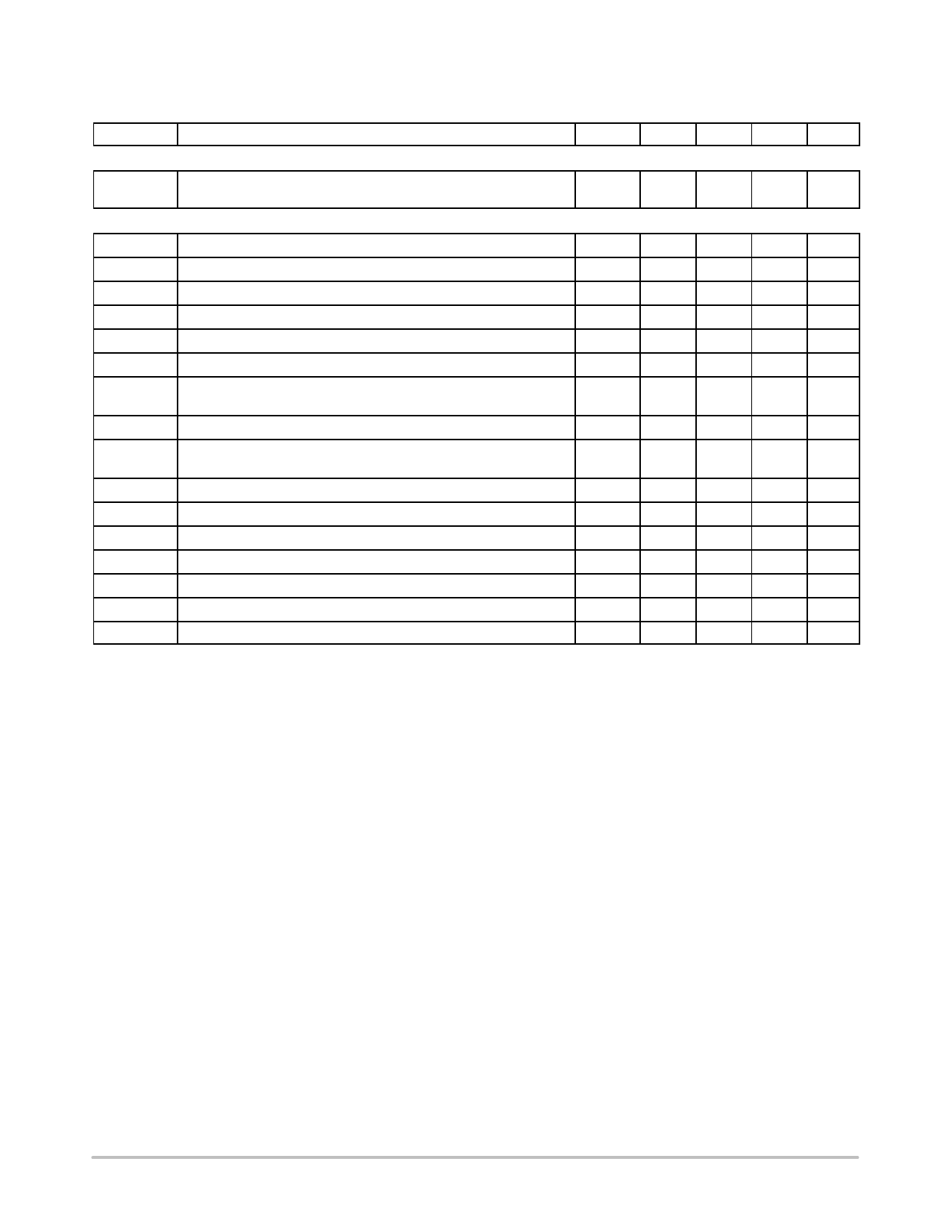
Electrical Characteristics
(For typical values Tj = 25°C, for min/max values Tj = −40°C to +125°C, Vcc = 15 V unless otherwise noted)
Symbol
Rating
Pin
Min
Typ
Max Unit
TIMERS
PFC_del
Internal delay timer after brown−out confirmation,
EN2 released or Vcc restart
−
−
100
−
ms
PROTECTIONS
VEN1
Reference voltage for the enable 1 input (latch), (Note 14), (Note 17)
10
0.95
1
1.05
V
VEN2
Reference voltage for the enable 2 input (Note 17)
11
0.95
1
1.05
V
HysteENX
Hysteresis for EN1, EN2 inputs
10, 11
−
50
−
mV
VdelEN1
Delay before latch confirmation on EN1 input (Note 14)
10
−
50
−
ms
VdelEN2
Delay between the EN2 activation and driver disable
11
−
80
120
ns
VBO
Brown−Out level
1
0.95
1
1.05
V
IBO
IBObias
Hysteresis current, Vpin 1 = 0.9 V, 0°C < TJ < 125°C
Hysteresis current, Vpin 1 = 0.9 V, −40°C < TJ < 125°C
Brown−Out input bias current
1
17.85
21
24.15 mA
16.31
21
24.15
1
−
0.02
−
mA
OTPref_I
OTPref_V
OTP Reference current (Note 16), 0°C < TJ < 125°C
OTP Reference current (Note 16), −40°C < TJ < 125°C
OTP reference voltage (Note 14), (Note 18)
8
155.7 173 190.3 mA
143.7 173 190.3
8
1.425 1.5
1.575
V
OTP_hyste
OTP comparator hysteresis
8
−
50
−
mV
OTPnoise
Noise filter on the OTP output (Note 14)
8
−
50
−
ms
FB_Fault
Above this level, the FB fault timer is activated (Note 15)
7
−
6
−
V
FB_timer
FB timeout duration (Note 15)
7
−
50
−
ms
TSD
Temperature shutdown threshold
−
140
−
−
°C
TSDhyste
Temperature shutdown hysteresis
−
−
30
−
°C
4. VCC(min) = VCCreset
5. Outputs Lgs and Hgs (pin 9/10) are unloaded.
6. Guaranteed by design.
7. DCsh = (DChs/(DChs + DCls)) * 100%, DCsl = (DCls/(DChs + DCls)) * 100%
8. The VFB_DC_0 is the FB voltage below which are all outputs disabled.
The FB voltage has to increases to VFB_DC_0 + VFB_DC_0_Hyste to re−enable all outputs of the controller.
9. Low impedance source and sink RDS(on) are designed to respectively deliver 0.5 A and −1 A at Tj = 100°C.
10. Pins 17, 18 and 19 are on the same potencial during IHV_LEAK measurements
11. On−time on synchro outputs wont be longer than on−time on power outputs.
12. The soft start pin is pulled down by an internal switch until the CIG timer ending voltage is reached
13. FB timer is disabled until the soft−start ending voltage is reached
14. EN1 input is blanked until the preheat period (CIG) ends. The OTP input is blanked during full startup sequence made of: PFC_del + CIG_t + SS_t
15. The FB timeout circuit starts to operate at the end of PFC_del + CIG_t + SS_t period.
16. An NTC resistor of 8.8 kW @ TA = 110°C is connected to ground.
17. The EN1 and EN2 input voltages have to go 50 mV below VEN1, VEN2 to release these inputs.
18. The OTP input voltage has to go 50 mV above OTPref_V to release this input.
19. The R_Fmin pin do not accept any bypass capacitor
20. Maximum acceptable capacitance connected to the pin is 100 pF
21. Measured for VCC = 10.5 V
http://onsemi.com
8
Share Link: