SCY99080CDWR2G 데이터 시트보기 (PDF) - ON Semiconductor
부품명
상세내역
일치하는 목록
SCY99080CDWR2G
ON Semiconductor

SCY99080CDWR2G Datasheet PDF : 27 Pages
| |||
DDA002C
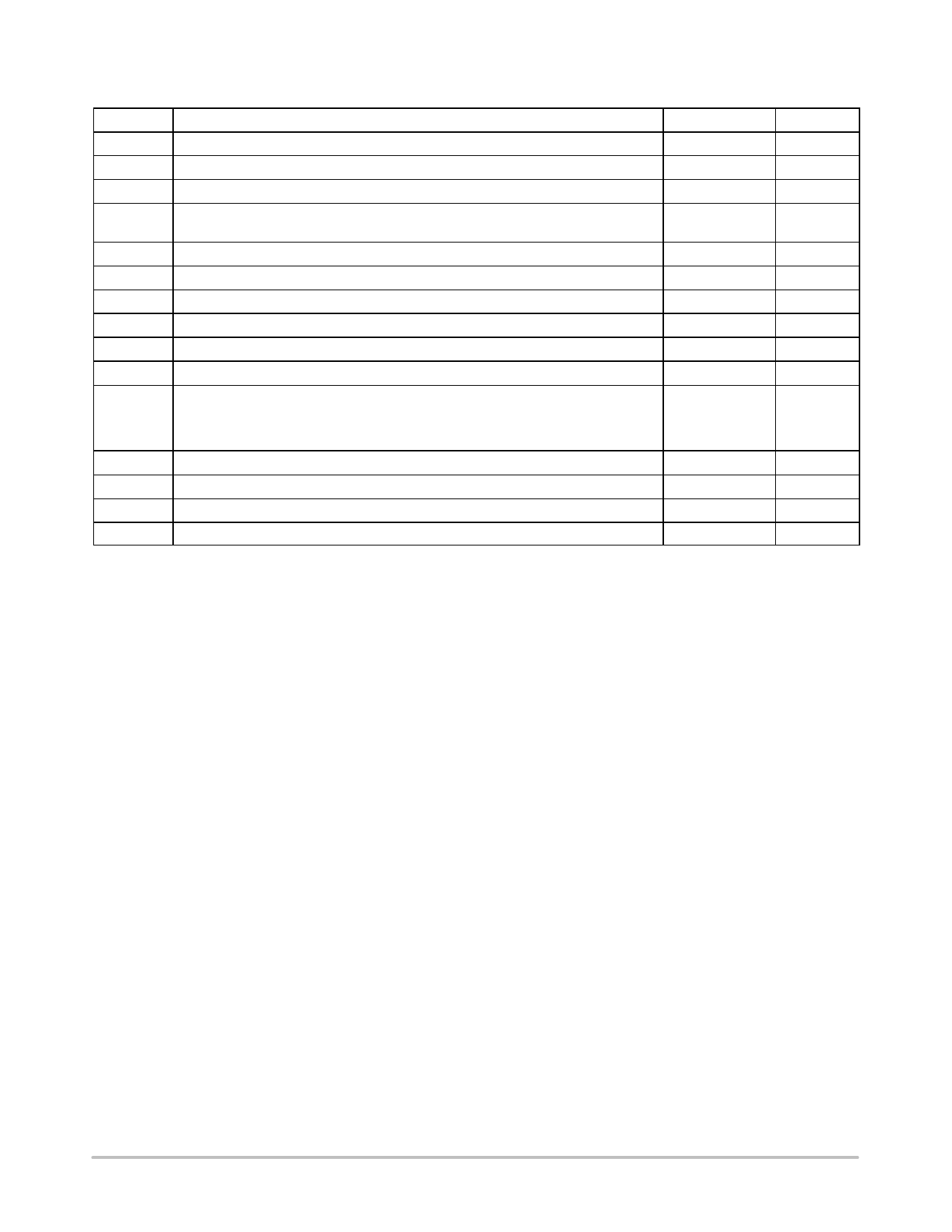
Maximum Ratings
Symbol
Rating
Value
Unit
VHB
Qmax
VBOOT−VHB
VHgd
Continuous voltage on the bridge pin, pin 17
Maximum injected charge into the HB pin (Note 3)
Floating supply voltage, pin 17 and 19
High side output voltage, pin 18
−1 to 600
V
11
nC
−0.3 to 20
V
VHB−0.3 to
V
VBOOT+0.3
VLgd
dVHB/dt
Vcc
Low side output voltage, pin 15
Maximum slew rate on the HB pin, pin 17
Power Supply voltage, pin 16
−0.3 to Vcc+0.3
±50
−0.3 to 20
V
V/ns
V
pin voltage, all pins (except pin 3, 6, 15, 16, 17, 18, and 19)
−0.3 to 10
V
VDgs
VR_Fmax
RqJ−A
Synchronous clamp pin voltage, pin 3
Maximum frequency adjust pin voltage, pin 6
Thermal Resistance Junction−to−Ambient,
(Soldered on traces with total area of 50 mm2, 1 oz copper)
Thermal Resistance Junction−to−Ambient,
(Soldered on recommended layout, 1 oz copper)
−0.3 to 5
−0.3 to 5
137
117
V
V
°C/W
Storage Temperature Range
−60 to +150
°C
TJmax
Maximum Junction Temperature
+150
°C
ESD Capability, HBM model (Except all HV pins i.e., HB, Hgd and Boot) (Note 1)
2
kV
ESD Capability, Machine Model
200
V
Stresses exceeding Maximum Ratings may damage the device. Maximum Ratings are stress ratings only. Functional operation above the
Recommended Operating Conditions is not implied. Extended exposure to stresses above the Recommended Operating Conditions may affect
device reliability.
1. This device series contains ESD protection and exceeds the following tests: Human Body Model 2000 V per JEDEC (22A114C − Human
Body Model and 22A115A Machine Model)
2. This device contains latch−up protection and exceeds 100 mA per JEDEC Standard JESD78.
3. The maximum injected charge corresponds to the injected current integrated over time into the half−bridge pin. Please refer to Figure 60
and related notes.
http://onsemi.com
5
Share Link: