SCY99080CDWR2G 데이터 시트보기 (PDF) - ON Semiconductor
부품명
상세내역
일치하는 목록
SCY99080CDWR2G
ON Semiconductor

SCY99080CDWR2G Datasheet PDF : 27 Pages
| |||
DDA002C
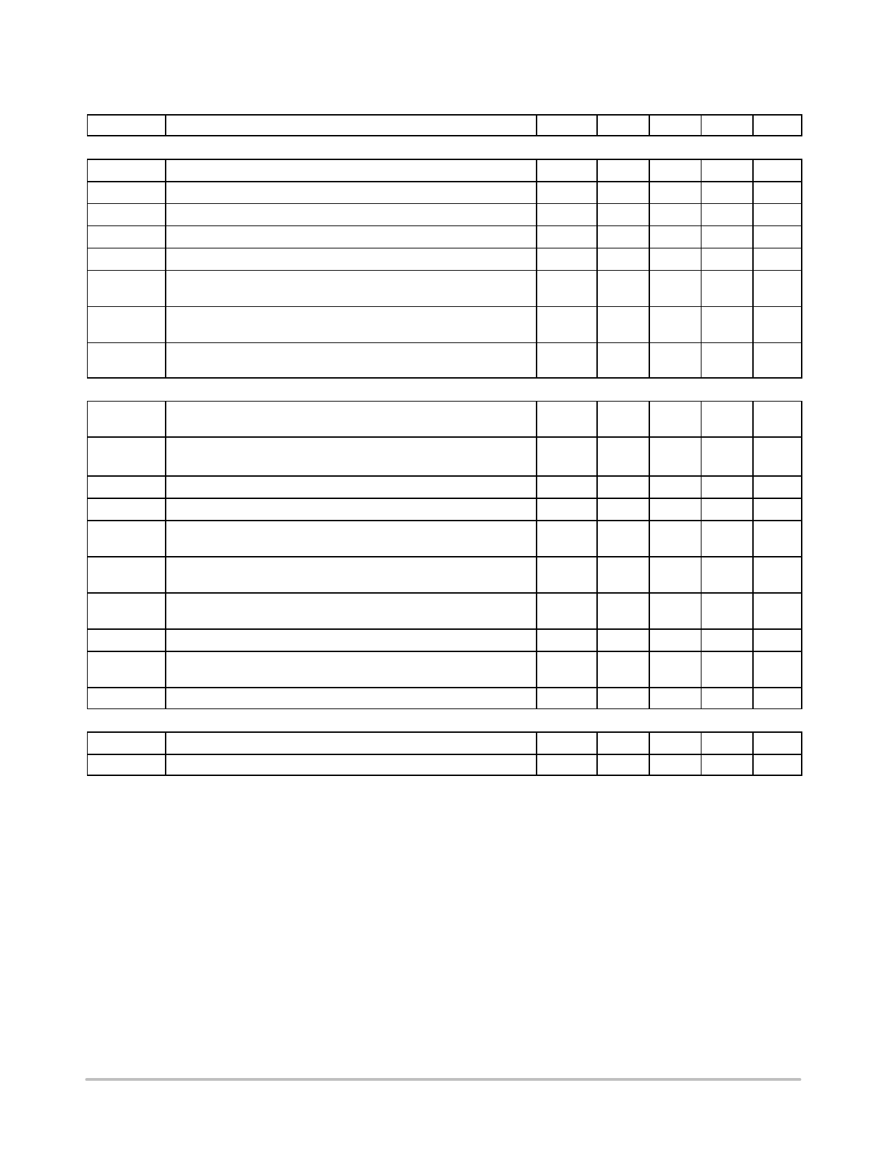
Electrical Characteristics
(For typical values Tj = 25°C, for min/max values Tj = −40°C to +125°C, Vcc = 15 V unless otherwise noted)
Symbol
Rating
Pin
Min
Typ
Max Unit
SUPPLY SECTION
VCCON
VCC(min)
VbootON
Vboot(min)
Istartup
ICC1
Turn−on threshold level, Vcc going up
Minimum operating voltage after turn−on (Note 4)
Startup voltage on the floating section
Cutoff voltage on the floating section
Startup current, Vcc < VCCON
Internal IC consumption, no output load on pin 18/17 – 15/14,
Fsw = 300 kHz (Note 5)
16
11
12
13
V
16
8.5
9.5
10.5
V
19,17
8
9
10
V
19,17
7.4
8.4
9.4
V
16
−
−
300
mA
16
−
5
−
mA
ICC2
Internal IC consumption, 1 nF output load on pin 18/17 – 15/14,
16
−
14
−
mA
Fsw = 300 kHz (Note 5)
ICC3
Internal IC consumption in fault mode
16
−
2.5
−
mA
(All drivers disabled, VCC > VCC(min))
VOLTAGE CONTROL OSCILLATOR (VCO)
Fsw min
Minimum switching frequency, R_Fmin = 41 kΩ on pin 5,
Vpin 7 > 5.5 V, DT = 300 ns (Notes 19 and 21)
5
58
60
62
kHz
Fsw max
Maximum switching frequency, R_Fmax = 2.5 kΩ on pin 6,
Vpin 7 < 1.2 V, DT = 100 ns, Rt = 41 kΩ (Notes 20 and 21)
6
450
500
550
kHz
SVCO
Maximum VCO conversion slope, Df / ΔVfb (Note 6)
−
−
120
− kHz / V
FBSW min
Feedback pin swing above which Df = 0, Fsw = Fmin, DC = 50%
7
−
5.1
−
V
FBSW max Feedback pin swing below which Df = 0, Fsw = Fmax, DC = 50%
7
(Note 6)
−
1.2
−
V
DCsl, DCsh
Operating duty−cycle symetry, 5.5 V> Vpin 7 > 0.5 V (Note 7)
18,17;
48
50
52
%
15,14
Min Ton
Minimum On time
18,17;
−
880
−
ns
15,14
VFB_DC_0
Skip comparator threshold on the feedback pin (Note 8)
7
−
1.2
−
V
VFB_DC_0_
Hyste
Hysteresis on the skip comparator
7
−
50
−
mV
VREF
Reference voltage for Fmin current generation
5
−
2
−
V
FEEDBACK SECTION
Rfb
Internal pull−up resistor
7
−
10
−
kΩ
Vfb_O
Open−loop voltage on the feedback pin, no optocoupler connection
7
−
7.3
−
V
4. VCC(min) = VCCreset
5. Outputs Lgs and Hgs (pin 9/10) are unloaded.
6. Guaranteed by design.
7. DCsh = (DChs/(DChs + DCls)) * 100%, DCsl = (DCls/(DChs + DCls)) * 100%
8. The VFB_DC_0 is the FB voltage below which are all outputs disabled.
The FB voltage has to increases to VFB_DC_0 + VFB_DC_0_Hyste to re−enable all outputs of the controller.
9. Low impedance source and sink RDS(on) are designed to respectively deliver 0.5 A and −1 A at Tj = 100°C.
10. Pins 17, 18 and 19 are on the same potencial during IHV_LEAK measurements
11. On−time on synchro outputs wont be longer than on−time on power outputs.
12. The soft start pin is pulled down by an internal switch until the CIG timer ending voltage is reached
13. FB timer is disabled until the soft−start ending voltage is reached
14. EN1 input is blanked until the preheat period (CIG) ends. The OTP input is blanked during full startup sequence made of: PFC_del + CIG_t + SS_t
15. The FB timeout circuit starts to operate at the end of PFC_del + CIG_t + SS_t period.
16. An NTC resistor of 8.8 kW @ TA = 110°C is connected to ground.
17. The EN1 and EN2 input voltages have to go 50 mV below VEN1, VEN2 to release these inputs.
18. The OTP input voltage has to go 50 mV above OTPref_V to release this input.
19. The R_Fmin pin do not accept any bypass capacitor
20. Maximum acceptable capacitance connected to the pin is 100 pF
21. Measured for VCC = 10.5 V
http://onsemi.com
6
Share Link: