MAX192ACAP 데이터 시트보기 (PDF) - Maxim Integrated
부품명
상세내역
일치하는 목록
MAX192ACAP Datasheet PDF : 24 Pages
| |||

Low-Power, 8-Channel,
Serial 10-Bit ADC
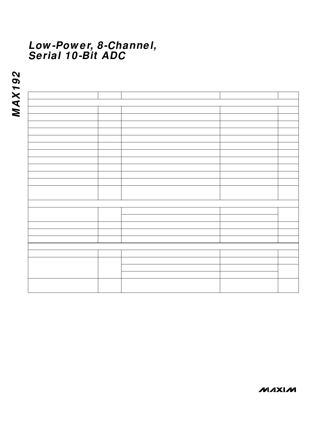
ELECTRICAL CHARACTERISTICS (continued)
(VDD = 5V ±5%, fCLK = 2.0MHz, external clock (50% duty cycle), 15 clocks/conversion cycle (133ksps), 4.7µF capacitor at VREF pin,
TA = TMIN to TMAX, unless otherwise noted. Typical values are at TA = +25°C.)
PARAMETER
SYMBOL
EDXIGTIETRANLAINLPRUETFSE(RDEINN,CSECALKT ,R–C—ES–F,A–S—DH—JD—N–)
DIN,SCLK, CS Input High Voltage
DIN,SCLK, CS Input Low Voltage
DIN, SCLK, CS Input Hysteresis
DIN, SCLK, CS Input Leakage
DIN, SCLK, CS Input Capacitance
SHDN Input High Voltage
SHDN Input Low Voltage
SHDN Input Current, High
SHDN Input Current, Low
SHDN Input Mid Voltage
SHDN Voltage, Floating
VINH
VINL
VHYST
IIN
CIN
VINH
VINL
IINH
IINL
VIM
VFLT
SHDN Max Allowed Leakage,
Mid Input
CONDITIONS
VIN = 0V or VDD
(Note 5)
SHDN = VDD
SHDN = 0V
SHDN = open
SHDN = open
DIGITAL OUTPUTS (DOUT, SSTRB)
Output Voltage Low
VOL
Output Voltage High
Three-State Leakage Current
Three-State Leakage Capacitance
POWER REQUIREMENTS
Positive Supply Voltage
VOH
IL
COUT
VDD
Positive Supply Current
IDD
ISINK = 5mA
ISINK = 16mA
ISOURCE = 1mA
CS = 5V
CS = 5V (Note 5)
Operating mode
Fast power-down
Full power-down
Positive Supply Rejection
(Note 9)
PSR
VDD = 5V ±5%; external reference, 4.096V;
full-scale input
MIN TYP MAX UNITS
2.4
V
0.8
V
0.15
V
±1
µA
15
pF
VDD - 0.5
V
0.5
V
4.0
µA
-4.0
µA
1.5
VDD - 1.5 V
2.75
V
-100
100
nA
0.4
V
0.3
4
V
±10
µA
15
pF
5 ±5%
V
1.5
2.5
mA
30
70
µA
2
10
±0.06 ±0.5 mV
Note 1: Tested at VDD = 5.0V; single-ended, unipolar.
Note 2: Relative accuracy is the deviation of the analog value at any code from its theoretical value after the full-scale range has
been calibrated.
Note 3: Grounded on-channel; sine wave applied to all off channels.
Note 4: Conversion time defined as the number of clock cycles times the clock period; clock has 50% duty cycle.
Note 5: Guaranteed by design. Not subject to production testing.
Note 6: The common-mode range for the analog inputs is from AGND to VDD.
Note 7: Sample tested to 0.1% AQL.
Note 8: External load should not change during conversion for specified accuracy.
Note 9: Measured at VSUPPLY + 5% and VSUPPLY - 5% only.
4 _______________________________________________________________________________________