MAX192ACAP 데이터 시트보기 (PDF) - Maxim Integrated
부품명
상세내역
일치하는 목록
MAX192ACAP Datasheet PDF : 24 Pages
| |||
Low-Power, 8-Channel,
Serial 10-Bit ADC
VDD
DGND
AGND
0V TO
4.096V
ANALOG 0.01µF
INPUT
MAX192
CH7
AGND
CS
SCLK
DIN
REFADJ
DOUT
SSTRB
C2
0.01µF
C1
4.7µF
VREF
SHDN
+2.5V +2.5V **
REFERENCE
+5V
N.C.
+5V
0.1µF
2MHz
OSCILLATOR
* FULL-SCALE ANALOG INPUT, CONVERSION RESULT = $FFF (HEX)
**OPTIONAL. A POTENTIOMETER MAY BE USED IN PLACE OF THE REFERENCE FOR TEST PURPOSES.
OSCILLOSCOPE
SCLK
SSTRB
DOUT*
CH1
CH2
CH3
CH4
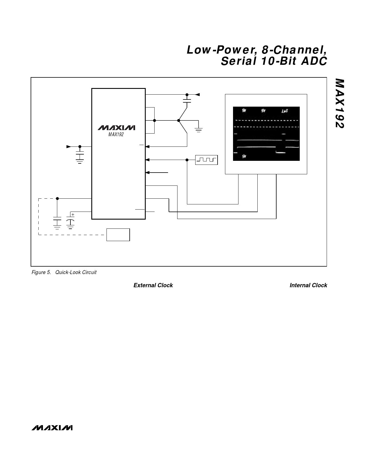
Figure 5. Quick-Look Circuit
External Clock
In external clock mode, the external clock not only
shifts data in and out, it also drives the analog-to-digital
conversion steps. SSTRB pulses high for one clock
period after the last bit of the control byte.
Successive-approximation bit decisions are made and
appear at DOUT on each of the next 12 SCLK falling
edges (see Figure 6). The first 10 bits are the true data
bits, and the last two are sub-LSB bits.
SSTRB and DOUT go into a high-impedance state when
CS goes high; after the next CS falling edge, SSTRB will
output a logic low. Figure 8 shows the SSTRB timing in
external clock mode.
The conversion must complete in some minimum time, or
else droop on the sample-and-hold capacitors may
degrade conversion results. Use internal clock mode if the
clock period exceeds 10µs, or if serial-clock interruptions
could cause the conversion interval to exceed 120µs.
Internal Clock
In internal clock mode, the MAX192 generates its own
conversion clock internally. This frees the microproces-
sor from the burden of running the SAR conversion
clock, and allows the conversion results to be read
back at the processor’s convenience, at any clock rate
from zero to typically 10MHz. SSTRB goes low at the
start of the conversion and then goes high when the
conversion is complete. SSTRB will be low for a maxi-
mum of 10µs, during which time SCLK should remain
low for best noise performance. An internal register
stores data when the conversion is in progress. SCLK
clocks the data out at this register at any time after the
conversion is complete. After SSTRB goes high, the
next falling clock edge will produce the MSB of the
conversion at DOUT, followed by the remaining bits in
MSB-first format (Figure 9). CS does not need to be
held low once a conversion is started.
______________________________________________________________________________________ 11
Share Link: 