NCP1547 데이터 시트보기 (PDF) - ON Semiconductor
부품명
상세내역
일치하는 목록
NCP1547 Datasheet PDF : 15 Pages
| |||
NCP1547
Startup
During power up, the regulator tends to quickly charge up
the output capacitors to reach voltage regulation. This gives
rise to an excessive in−rush current which can be detrimental
to the inductor, IC and catch diode. In V2 control , the
compensation capacitor provides Soft−Start with no need
for extra pin or circuitry. During the power up, the Output
Source Current of the error amplifier charges the
compensation capacitor which forces VC pin and thus output
voltage ramp up gradually. The Soft−Start duration can be
calculated by
TSS
+
VC CCOMP
ISOURCE
where:
VC = VC pin steady−state voltage, which is approximately
equal to error amplifier’s reference voltage.
CCOMP = Compensation capacitor connected to the VC pin
ISOURCE = Output Source Current of the error amplifier.
Using a 0.1 mF CCOMP, the calculation shows a TSS over
5.0 ms which is adequate to avoid any current stresses.
Figure 11 shows the gradual rise of the VC, VO and envelope
of the VSW during power up. There is no voltage over−shoot
after the output voltage reaches the regulation. If the supply
voltage rises slower than the VC pin, output voltage may
over−shoot.
Figure 11. The Power Up Transition of NCP1547
Regulator
Short Circuit
When the VFB pin voltage drops below Foldback
Threshold, the regulator reduces the peak current limit by
40% and switching frequency to 1/4 of the nominal
frequency. These features are designed to protect the IC and
external components during over load or short circuit
conditions. In those conditions, peak switching current is
clamped to the current limit threshold. The reduced
switching frequency significantly increases the ripple
current, and thus lowers the DC current. The short circuit can
cause the minimum duty cycle to be limited by Minimum
Output Pulse Width. The foldback frequency reduces the
minimum duty cycle by extending the switching cycle. This
protects the IC from overheating, and also limits the power
that can be transferred to the output. The current limit
foldback effectively reduces the current stress on the
inductor and diode. When the output is shorted, the DC
current of the inductor and diode can approach the current
limit threshold. Therefore, reducing the current limit by 40%
can result in an equal percentage drop of the inductor and
diode current. The short circuit waveforms are captured in
Figure 12, and the benefit of the foldback frequency and
current limit is self−evident.
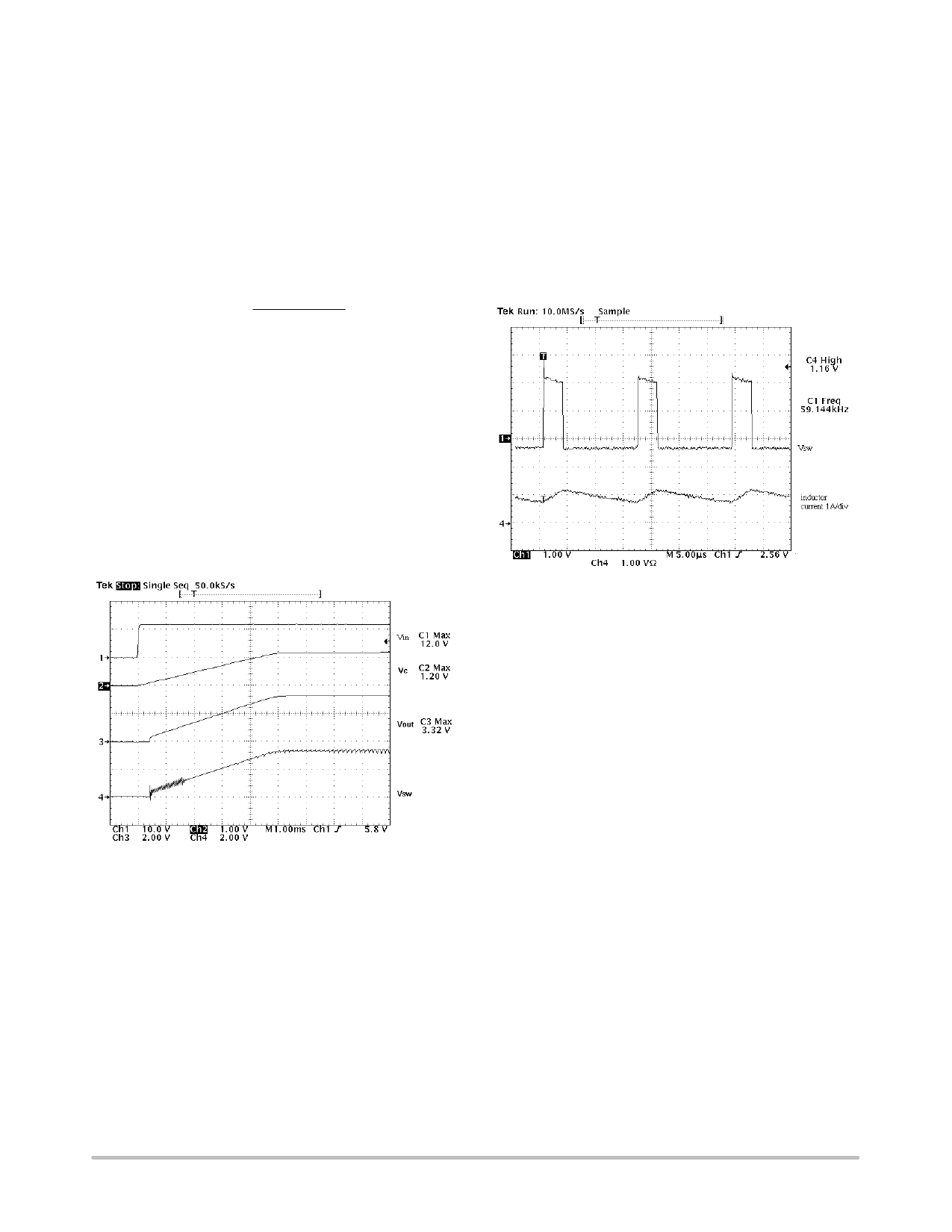
Figure 12. In Short Circuit, the Foldback Current and
Foldback Frequency Limit the Switching Current to
Protect the IC, Inductor and Catch Diode
Thermal Considerations
A calculation of the power dissipation of the IC is always
necessary prior to the adoption of the regulator. The current
drawn by the IC includes quiescent current, pre−driver
current, and power switch base current. The quiescent
current drives the low power circuits in the IC, which
include comparators, error amplifier and other logic blocks.
Therefore, this current is independent of the switching
current and generates power equal to
WQ + VIN IQ
where:
IQ = quiescent current.
The pre−driver current is used to turn on/off the power
switch and is approximately equal to 12 mA in worst case.
During steady state operation, the IC draws this current from
the Boost pin when the power switch is on and then receives
it from the VIN pin when the switch is off. The pre−driver
current always returns to the VSW pin. Since the pre−driver
current goes out to the regulator’s output even when the
power switch is turned off, a minimum load is required to
prevent overvoltage in light load conditions. If the Boost pin
voltage is equal to VIN + VO when the switch is on, the power
dissipation due to pre−driver current can be calculated by
http://onsemi.com
9
Share Link: 