NCP1547 데이터 시트보기 (PDF) - ON Semiconductor
부품명
상세내역
일치하는 목록
NCP1547 Datasheet PDF : 15 Pages
| |||
NCP1547
oscillation, as shown in Figure 8. Similar to current mode
control, this oscillation occurs at the duty cycle greater than
50% and can be alleviated by using a larger inductor value.
The current limit threshold is reduced to Foldback Current
when the FB pin falls below Foldback Threshold. This
feature protects the IC and external components under the
power up or over−load conditions.
Figure 8. The Regulator in Current Limit
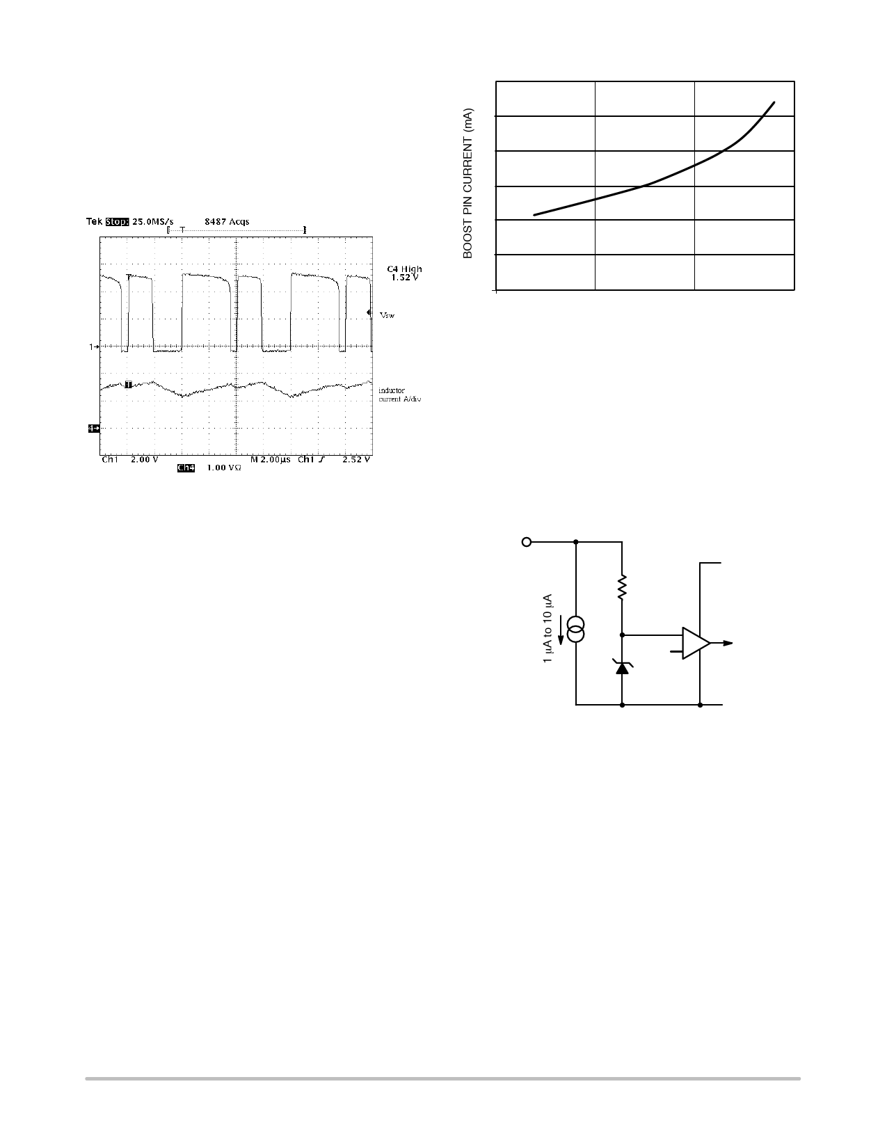
BOOST Pin
The BOOST pin provides base driving current for the
power switch. A voltage higher than VIN provides required
headroom to turn on the power switch. This in turn reduces
IC power dissipation and improves overall system
efficiency. The BOOST pin can be connected to an external
boost−strapping circuit which typically uses a 0.1 mF capacitor
and a 1N914 or 1N4148 diode, as shown in Figure 1.
When the power switch is turned on, the voltage on the
BOOST pin is equal to
VBOOST + VIN ) VO * VF
where:
VF = diode forward voltage.
The anode of the diode can be connected to any DC
voltage as well as the regulated output voltage (Figure 1).
However, the maximum voltage on the BOOST pin shall not
exceed 40 V.
As shown in Figure 9, the BOOST pin current includes a
constant 7.0 mA pre−driver current and base current
proportional to switch conducting current. A detailed
discussion of this current is conducted in Thermal
Consideration section. A 0.1 mF capacitor is usually
adequate for maintaining the Boost pin voltage during the on
time.
30
25
20
15
10
5
00
0.5
1.0
1.5
SWITCHING CURRENT (A)
Figure 9. The Boost Pin Current Includes 7.0 mA
Pre−Driver Current and Base Current when the
Switch is Turned On. The Beta Decline of the
Power Switch Further Increases the Base
Current at High Switching Current
Shutdown
The internal power switch will not turn on until the VIN
pin rises above the Startup Voltage. This ensures no
switching will occur until adequate supply voltage is
provided to the IC. Refer to Figure 10 for the SHDNB
(shutdown−bar) pin input circuit.
SHDNB
VIN
20k
±33%
-
1.2V +
VZ = 6V to 8V
Figure 10.
GND
The IC enters a sleep mode when the SHDNB pin is pulled
below the Shutdown Threshold Voltage. In sleep mode, the
power switch is kept open and the supply current reduces to
Shutdown Quiescent Current (1 mA typically). This pin has
an internal pull−down current. When not in use, pull this pin
up to VCC with a resistor (See Figure 1). A 100 kW pullup
resistor will ensure safe operation from below 9 V and
during a 40 V load dump condition.
http://onsemi.com
8
Share Link: 