NCP1547 데이터 시트보기 (PDF) - ON Semiconductor
부품명
상세내역
일치하는 목록
NCP1547 Datasheet PDF : 15 Pages
| |||
NCP1547
WDRV + 12 mA (VIN * VO ) VVOIN2)
The base current of a bipolar transistor is equal to collector
current divided by beta of the device. Beta of 60 is used here
to estimate the base current. The Boost pin provides the base
current when the transistor needs to be on. The power
dissipated by the IC due to this current is
WBASE
+
VO2
VIN
IS
60
where:
IS = DC switching current.
When the power switch turns on, the saturation voltage
and conduction current contribute to the power loss of a
non−ideal switch. The power loss can be quantified as
WSAT
+
VO
VIN
IS
VSAT
where:
VSAT = saturation voltage of the power switch which is
shown in Figure 7.
The switching loss occurs when the switch experiences
both high current and voltage during each switch transition.
This regulator has a 30 ns turn−off time and associated
power loss is equal to
WS + IS
VIN
2
30 ns
fS
The turn−on time is much shorter and thus turn−on loss is
not considered here.
The total power dissipated by the IC is sum of all the above
WIC + WQ ) WDRV ) WBASE ) WSAT ) WS
The IC junction temperature can be calculated from the
ambient temperature, IC power dissipation and thermal
resistance of the package. The equation is shown as follows,
TJ + WIC RqJA ) TA
Minimum Load Requirement
As pointed out in the previous section, a minimum load is
required for this regulator due to the pre−driver current
feeding the output. Placing a resistor equal to VO divided by
12 mA should prevent any voltage overshoot at light load
conditions. Alternatively, the feedback resistors can be
valued properly to consume 12 mA current.
COMPONENT SELECTION
Input Capacitor
In a buck converter, the input capacitor witnesses pulsed
current with an amplitude equal to the load current. This
pulsed current and the ESR of the input capacitors determine
the VIN ripple voltage, which is shown in Figure 13. For VIN
ripple, low ESR is a critical requirement for the input
capacitor selection. The pulsed input current possesses a
significant AC component, which is absorbed by the input
capacitors. The RMS current of the input capacitor can be
calculated using:
IRMS + IO ǸD(1 * D)
where:
D = switching duty cycle which is equal to VO/VIN.
IO = load current.
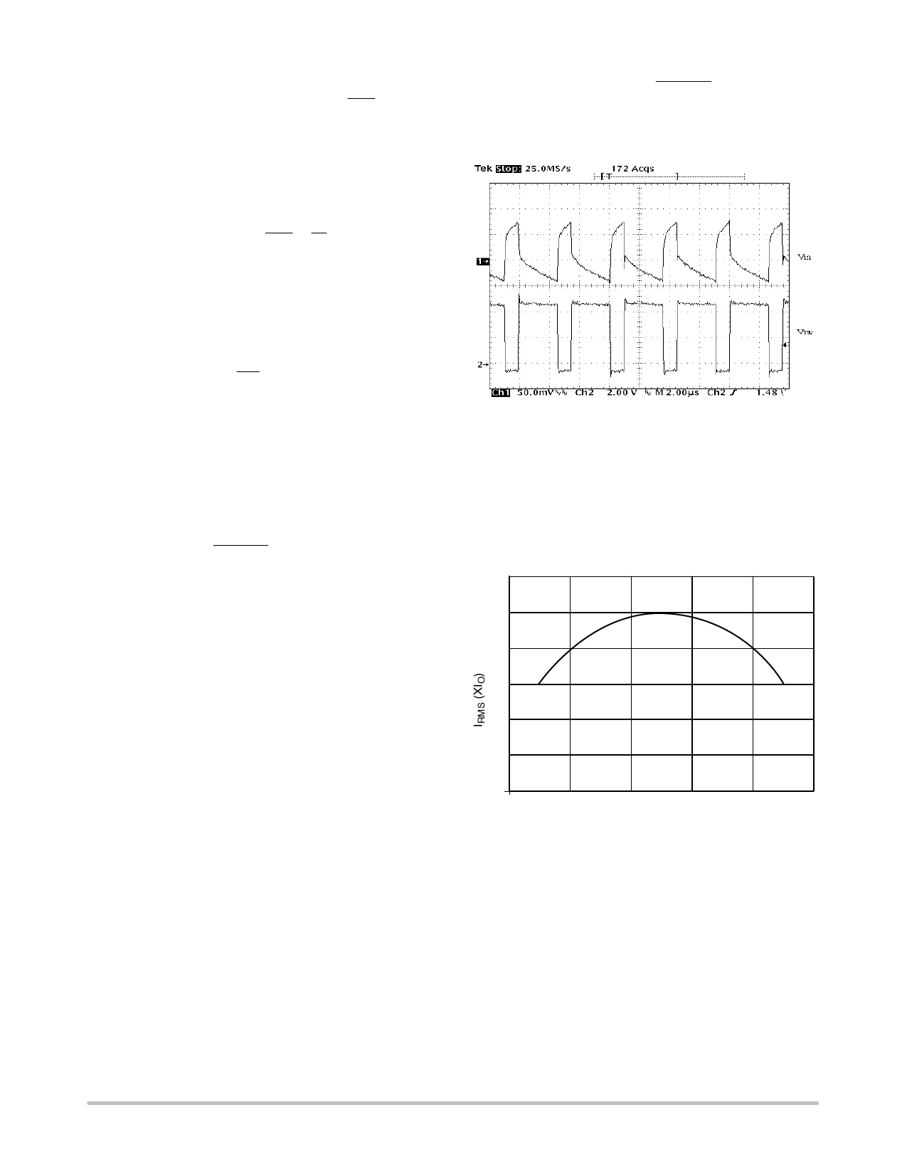
Figure 13. Input Voltage Ripple in a Buck Converter
To calculate the RMS current, multiply the load current
with the constant given by Figure 14 at each duty cycle. It is
a common practice to select the input capacitor with an RMS
current rating more than half the maximum load current. If
multiple capacitors are paralleled, the RMS current for each
capacitor should be the total current divided by the number
of capacitors.
0.6
0.5
0.4
0.3
0.2
0.1
00
0.2
0.4
0.6
0.8
1.0
DUTY CYCLE
Figure 14. Input Capacitor RMS Current can be
Calculated by Multiplying Y Value with Maximum Load
Current at any Duty Cycle
Selecting the capacitor type is determined by each
design’s constraint and emphasis. The aluminum
electrolytic capacitors are widely available at lowest cost.
Their ESR and ESL (equivalent series inductor) are
relatively high. Multiple capacitors are usually paralleled to
achieve lower ESR. In addition, electrolytic capacitors
usually need to be paralleled with a ceramic capacitor for
filtering high frequency noises. The OS−CON are solid
aluminum electrolytic capacitors, and therefore has a much
lower ESR. Recently, the price of the OS−CON capacitors
has dropped significantly so that it is now feasible to use
http://onsemi.com
10
Share Link: 