CY7C146-45JI 데이터 시트보기 (PDF) - Cypress Semiconductor
부품명
상세내역
일치하는 목록
CY7C146-45JI Datasheet PDF : 15 Pages
| |||
CY7C132, CY7C136
CY7C136A, CY7C142, CY7C146
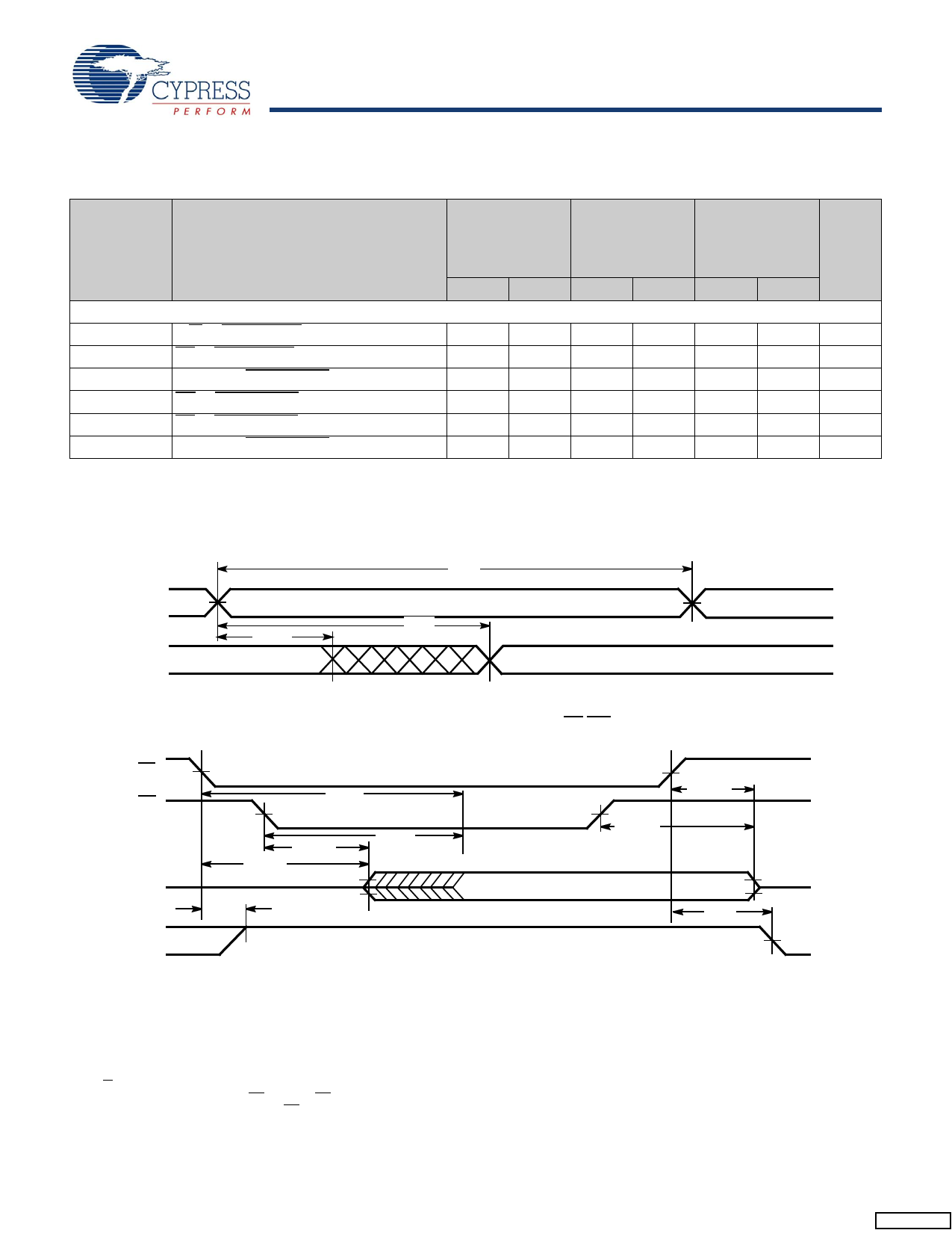
Switching Characteristics
Over the Operating Range (Speeds -35, -45, -55) [8] (continued)
Parameter
Description
Interrupt Timing [16]
tWINS
tEINS
tINS
tOINR
tEINR
tINR
R/W to INTERRUPT Set Time
CE to INTERRUPT Set Time
Address to INTERRUPT Set Time
OE to INTERRUPT Reset Time[13]
CE to INTERRUPT Reset Time[13]
Address to INTERRUPT Reset Time[13]
7C132-35
7C136-35
7C142-35
7C146-35
7C132-45
7C136-45
7C142-45
7C146-45
7C132-55
7C136-55
7C136A-55
7C142-55
Unit
7C146-55
Min
Max
Min
Max
Min
Max
25
35
45
ns
25
35
45
ns
25
35
45
ns
25
35
45
ns
25
35
45
ns
25
35
45
ns
Switching Waveforms
Figure 4. Read Cycle No. 1 (Either Port-Address Access) [17, 18]
ADDRESS
DATA OUT
tOHA
PREVIOUS DATA VALID
tRC
tAA
DATA VALID
CE
OE
DATA OUT
ICC
ISB
Figure 5. Read Cycle No. 2 (Either Port-CE/OE )[17, 19]
tACE
tLZCE
tLZOE
tDOE
tPU
tHZOE
tHZCE
DATA VALID
tPD
Notes
17. R/W is HIGH for read cycle.
18. Device is continuously selected, CE = VIL and OE = VIL.
19. Address valid prior to or coincident with CE transition LOW.
Document #: 38-06031 Rev. *E
Page 7 of 15
[+] Feedback
Share Link: 