PCA9540B 데이터 시트보기 (PDF) - Philips Electronics
부품명
상세내역
일치하는 목록
PCA9540B Datasheet PDF : 14 Pages
| |||
Philips Semiconductors
2-channel I2C multiplexer
Product data sheet
PCA9540B
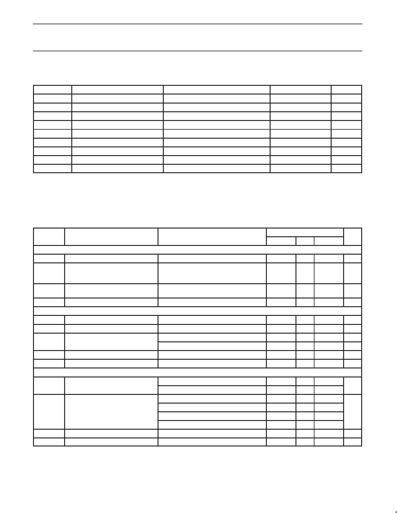
ABSOLUTE MAXIMUM RATINGS1, 2
In accordance with the Absolute Maximum Rating System (IEC 134).Voltages are referenced to GND (ground = 0 V).
SYMBOL
PARAMETER
CONDITIONS
RATING
UNIT
VDD
DC supply voltage
–0.5 to +7.0
V
VI
DC input voltage
–0.5 to +7.0
V
II
DC input current
±20
mA
IO
DC output current
±25
mA
IDD
Supply current
±100
mA
ISS
Supply current
±100
mA
Ptot
total power dissipation
400
mW
Tstg
Storage temperature range
–60 to +150
°C
Tamb
Operating ambient temperature
–40 to +85
°C
NOTES:
1. Stresses beyond those listed may cause permanent damage to the device. These are stress ratings only and functional operation of the
device at these or any other conditions beyond those indicated under “recommended operating conditions” is not implied. Exposure to
absolute-maximum-rated conditions for extended periods may affect device reliability.
2. The performance capability of a high-performance integrated circuit in conjunction with its thermal environment can create junction
temperatures which are detrimental to reliability. The maximum junction temperature of this integrated circuit should not exceed 150 °C.
DC CHARACTERISTICS
VDD = 2.3 to 3.6 V; VSS = 0 V; Tamb = –40 to +85 °C; unless otherwise specified. (See page 9 for VDD = 3.6 to 5.5 V)
SYMBOL
PARAMETER
TEST CONDITIONS
LIMITS
MIN
TYP
Supply
VDD
Supply voltage
IDD
Supply current
Operating mode; VDD = 3.6 V;
no load; VI = VDD or VSS;
fSCL = 100 kHz
2.3
—
—
20
Istb
Standby current
VPOR
Power-on reset voltage (Note 1)
Input SCL; input/output SDA
Standby mode; VDD = 3.6 V;
no load; VI = VDD or VSS; fSLC = 0 kHz
no load; VI = VDD or VSS
—
0.1
—
1.6
VIL
LOW-level input voltage
VIH
HIGH-level input voltage
IOL
LOW-level output current
IL
Ci
Pass Gate
Leakage current
Input capacitance
VOL = 0.4 V
VOL = 0.6 V
VI = VDD or VSS
VI = VSS
–0.5
—
0.7VDD
—
3
—
6
—
–1
—
—
7
RON
Switch resistance
VCC = 3.0 to 3.6 V, VO = 0.4 V, IO = 15 mA
5
11
VCC = 2.3 to 2.7 V, VO = 0.4 V, IO = 10 mA
7
16
Vswin = VDD = 3.3 V; Iswout = –100 µA
—
1.9
VPass
Switch output voltage
Vswin = VDD = 3.0 to 3.6 V; Iswout = –100 µA
1.6
—
Vswin = VDD = 2.5 V; Iswout = –100 µA
—
1.5
Vswin = VDD = 2.3 to 2.7 V; Iswout = –100 µA
1.1
—
IL
Leakage current
VI = VDD or VSS
–1
—
Cio
Input/output capacitance
NOTE:
1. VDD must be lowered to 0.2 V in order to reset part.
VI = VSS
—
2.5
MAX
3.6
50
1
2.1
0.3VDD
6
—
—
+1
8
31
55
—
2.8
—
2.0
+1
5
UNIT
V
µA
µA
V
V
V
mA
mA
µA
pF
Ω
V
µA
pF
2004 Sep 29
8
Share Link: 