PCA9540B 데이터 시트보기 (PDF) - Philips Electronics
부품명
상세내역
일치하는 목록
PCA9540B Datasheet PDF : 14 Pages
| |||
Philips Semiconductors
2-channel I2C multiplexer
Product data sheet
PCA9540B
FEATURES
• 1-of-2 bi-directional translating multiplexer
• I2C interface logic; compatible with SMBus standards
• Channel selection via I2C-bus
• Power up with all multiplexer channels deselected
• Low RdsON switches
• Allows voltage level translation between 1.8 V, 2.5 V, 3.3 V and
5 V buses
• No glitch on power-up
• Supports hot insertion
• Low stand-by current
• Operating power supply voltage range of 2.3 V to 5.5 V
• 5 V tolerant Inputs
• 0 to 400 kHz clock frequency
• ESD protection exceeds 2000 V HBM per JESD22-A114,
200 V MM per JESD22-A115 and 1000 V per JESD22-C101
• Latch-up testing is done to JESDEC Standard JESD78 which
exceeds 100 mA
• Packages Offered: SO8, TSSOP8
DESCRIPTION
The PCA9540B is a 1-of-2 bi-directional translating multiplexer,
controlled via the I2C-bus. The SCL/SDA upstream pair fans out to
two SCx/SDx downstream pairs, or channels. Only one SCx/SDx
channel is selected at a time, determined by the contents of the
programmable control register.
A power-on reset function puts the registers in their default state and
initializes the I2C state machine with no channels selected.
The pass gates of the multiplexer are constructed such that the VDD
pin can be used to limit the maximum high voltage which will be
passed by the PCA9540B. This allows the use of different bus
voltages on each SCx/SDx pair, so that 1.8 V, 2.5, or 3.3 V parts can
communicate with 5 V parts without any additional protection.
External pull-up resistors can pull the bus up to the desired voltage
level for this channel. All I/O pins are 5 V tolerant.
The PCA9540B has replaced the PCA9540 and all designs must
migrate to the PCA9540B. PCA9540B samples can be requested
from www.philipslogic.com/products/I2Cmuxes/.
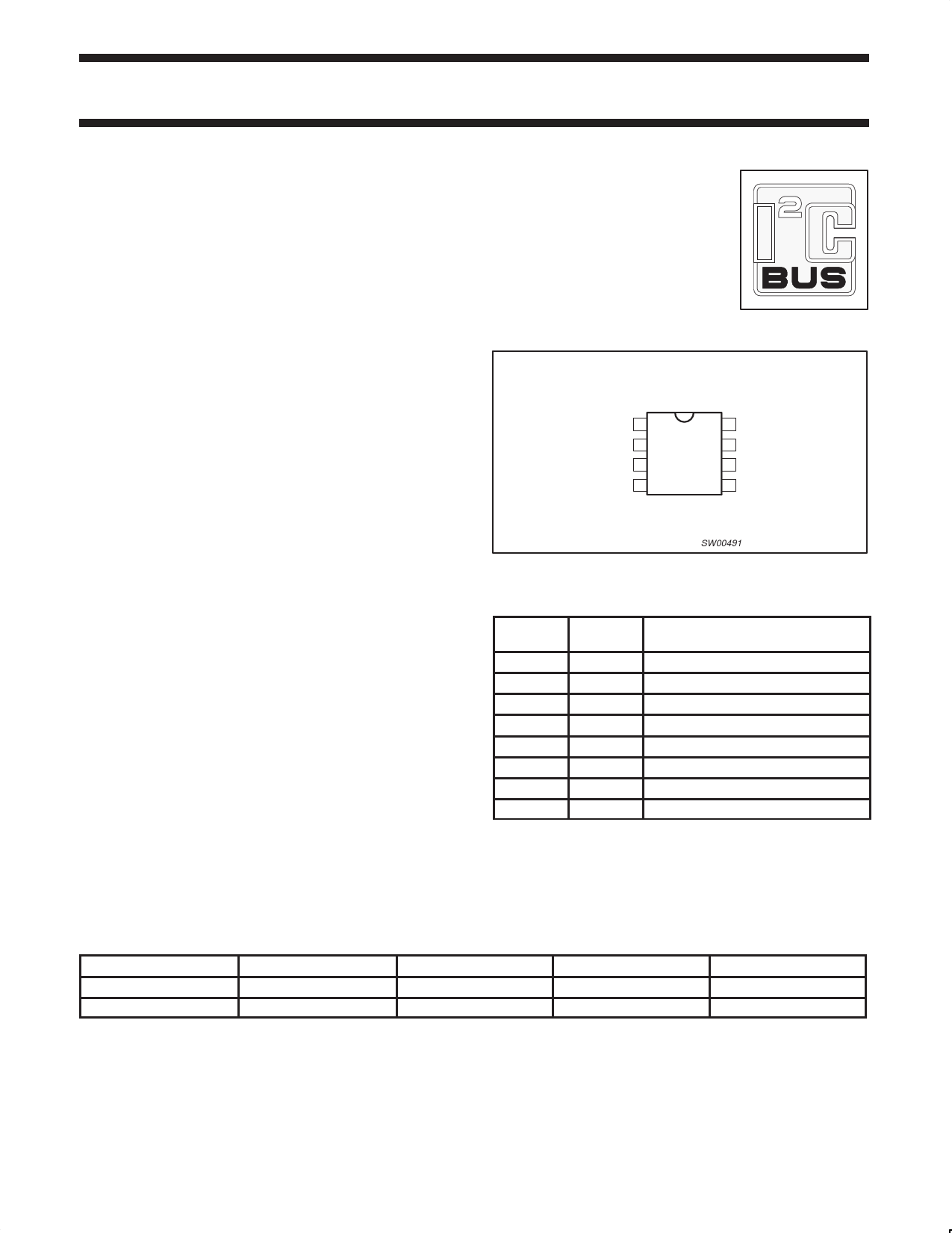
PIN CONFIGURATION
SCL 1
SDA 2
VDD 3
SD0 4
8 SC1
7 SD1
6 VSS
5 SC0
SW00491
Figure 1. Pin configuration
PIN DESCRIPTION
PIN
NUMBER
SYMBOL
1
SCL
2
SDA
3
VDD
4
SD0
5
SC0
6
VSS
7
SD1
8
SC1
FUNCTION
Serial clock line
Serial data line
Supply voltage
Serial data 0
Serial clock 0
Supply ground
Serial data 1
Serial clock 1
ORDERING INFORMATION
PACKAGES
TEMPERATURE RANGE
ORDER CODE
TOPSIDE MARK
DRAWING NUMBER
8-Pin Plastic SO
–40 °C to +85 °C
PCA9540BD
PA9540B
SOT96-1
8-Pin Plastic TSSOP
–40 °C to +85 °C
PCA9540BDP
9540B
Standard packing quantities and other packaging data are available at www.standardproducts.philips.com/packaging.
SOT505-1
2004 Sep 29
2
Share Link: 