A3G4250D 데이터 시트보기 (PDF) - STMicroelectronics
부품명
상세내역
일치하는 목록
A3G4250D Datasheet PDF : 44 Pages
| |||
Mechanical and electrical characteristics
A3G4250D
2.4
2.4.1
Communication interface characteristics
SPI - serial peripheral interface
Subject to general operating conditions for Vdd and Top.
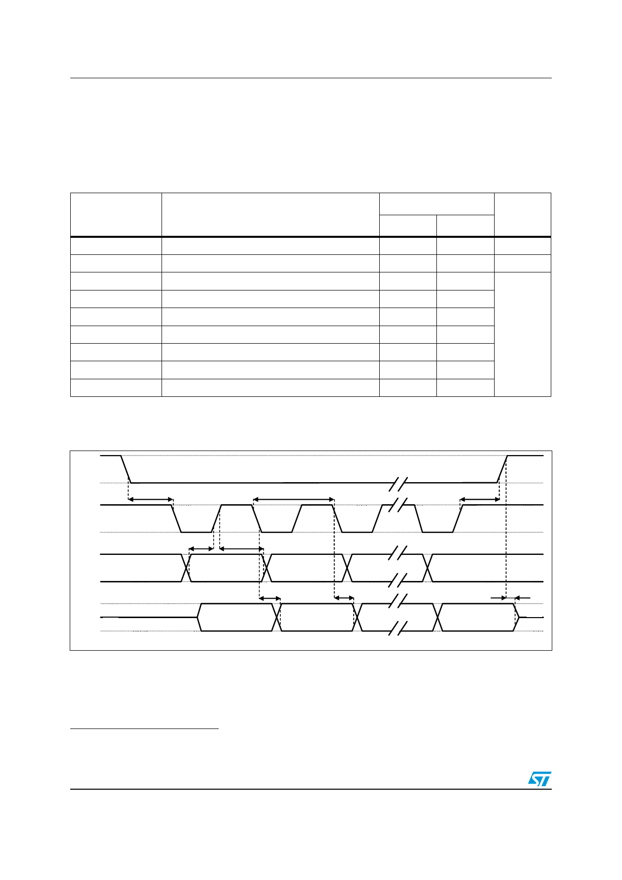
Table 7. SPI slave timing values
Symbol
Parameter
Value(1)
Min.
Max.
Unit
tc(SPC)
SPI clock cycle
100
ns
fc(SPC)
tsu(CS)
th(CS)
tsu(SI)
th(SI)
SPI clock frequency
CS setup time
CS hold time
SDI input setup time
SDI input hold time
10
MHz
5
8
5
15
ns
tv(SO)
th(SO)
tdis(SO)
SDO valid output time
SDO output hold time
SDO output disable time
50
6
50
1. Values are guaranteed at 10 MHz clock frequency for SPI with both 4 and 3 wires, based on characterization results; not
tested in production.
Figure 4. SPI slave timing diagram(e)
&6 �
WVX
&6
63& �
WVX
6,
WK
6,
WF
63&
WK
&6
6', �
06%,1
WY
62
WK
62
/6%,1
WGLV
62
6'2 �
06%287
/6%287
!-V
e. Measurement points are done at 0.2·Vdd_IO and 0.8·Vdd_IO, for both input and output ports.
12/44
Doc 022768 Rev 3
Share Link: 