NJU3101 데이터 시트보기 (PDF) - Japan Radio Corporation
부품명
상세내역
일치하는 목록
NJU3101 Datasheet PDF : 22 Pages
| |||
NJU3101
• DATA MEMORY(RAM)
DATA MEMORY(RAM) is formed with the 4-bit length a word. The NJU3101 prepares 16 words(64
bits) RAM. The data formed with the 4-bit length a word can be read/written from/to RAM, and the data
formed with the 1-bit length in a word can be set, reset, or tested by the bit-operation instruction.
The RAM address is indicated indirectly by Y-reg.
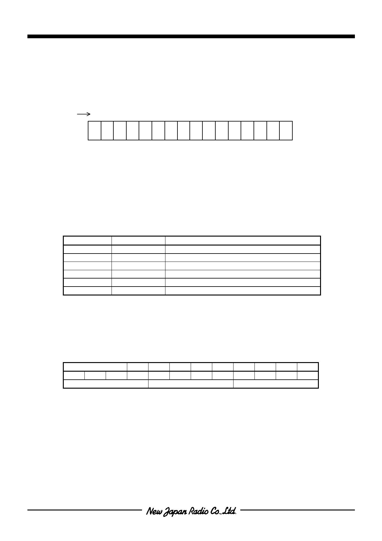
[RAM ADDRESS MAP]
Y-reg
0 1 2 3 4 5 6 7 8 9 A B C D E F [HEX]
• PERIPHERAL REGISTERs(PH)
PERIPHERAL REGISTERs(PH) controlling I/O Ports or the ROM address are selected by the data in
Y'-reg.
The Peripheral Register assigned for each I/O Port can get the signal data from the external application
by reading operation, or can output the signal data to the external application by writing operation in
accordance with the type of input or output selected by the mask option. Although the data can be read
from the Peripheral Register assigned as the Output, it sometimes takes the incorrect data of the Output
Port.
[PERIPHERAL REGISTER TABLE]
Y'-register
1H
2H
3H
4H
5H
DH
Register No.
PHY1
PHY2
PHY3
PHY4
PHY5
PHY13
Peripheral Register Name
PORTA Output or PORTA Input
PORTB Output or PORTB Input
PORTC Output or PORTC Input
PORTD Output or PORTD Input
PORTE Output or PORTE Input
ROM Addressing Register
• ROM ADDRESSING REGISTER(PHY13)
ROM ADDRESSING REGISTER(PHY13) indicates the address of ROM with Accumulator and X'-reg
for the data transference operation(TRM) from ROM to RAM. The effective bit on ROM Addressing
Register(PHY13) is b0, and the other three bits, b1, b2 and b3, are not related.
The PHY13 condition is unknown on “RESET” operation.
[ROM ADDRESSING]
no used
A8 A7 A6 A5 A4 A3 A2 A1 A0
b3 b2 b1 b0 b3 b2 b1 b0 b3 b2 b1 b0
PHY13
X'
AC
-7-
Share Link: 