NJU3101 데이터 시트보기 (PDF) - Japan Radio Corporation
부품명
상세내역
일치하는 목록
NJU3101 Datasheet PDF : 22 Pages
| |||
NJU3101
• PORTD(PD0, PD1)
PORTD is a 2-bit input-output PORT. When the PORT is set as the output, the signal is output through
the output terminal by writing data to the PORTD register(PHY4). When the PORT is set as the input,
the external signal is gotten directly through the input terminal by reading data from PHY4.
When this PORTD is set as the input, these two ports perform the extra functions as follows:
a) PD0 TERMINAL
PD0 TERMINAL performs the extra function as the restart signal input terminal to return from the
"STANDBY" mode. When the rising edge of the signal from the external circuit is input into the PD0
terminal in mode of "STANDBY", the "STANDBY" mode is released and the CPU starts the execution
again from the suspended address of the program. (refer !STANDBY FUNCTION)
b) PD1 TERMINAL
PD1 TERMINAL performs the extra function as the edge detector terminal. When the PD1 terminal
detects the edge of the signal from the external circuit, the third bit(b2) condition of PHY4 is set to "1".
The “b2” of PHY4 is set to “1” even when the edge is input during the “STANDBY” mode. The condition
of “b2” is kept until the writing operation to PHY4.
The polarity as low to high or high to low of the input signal edge can be selected by the mask option.
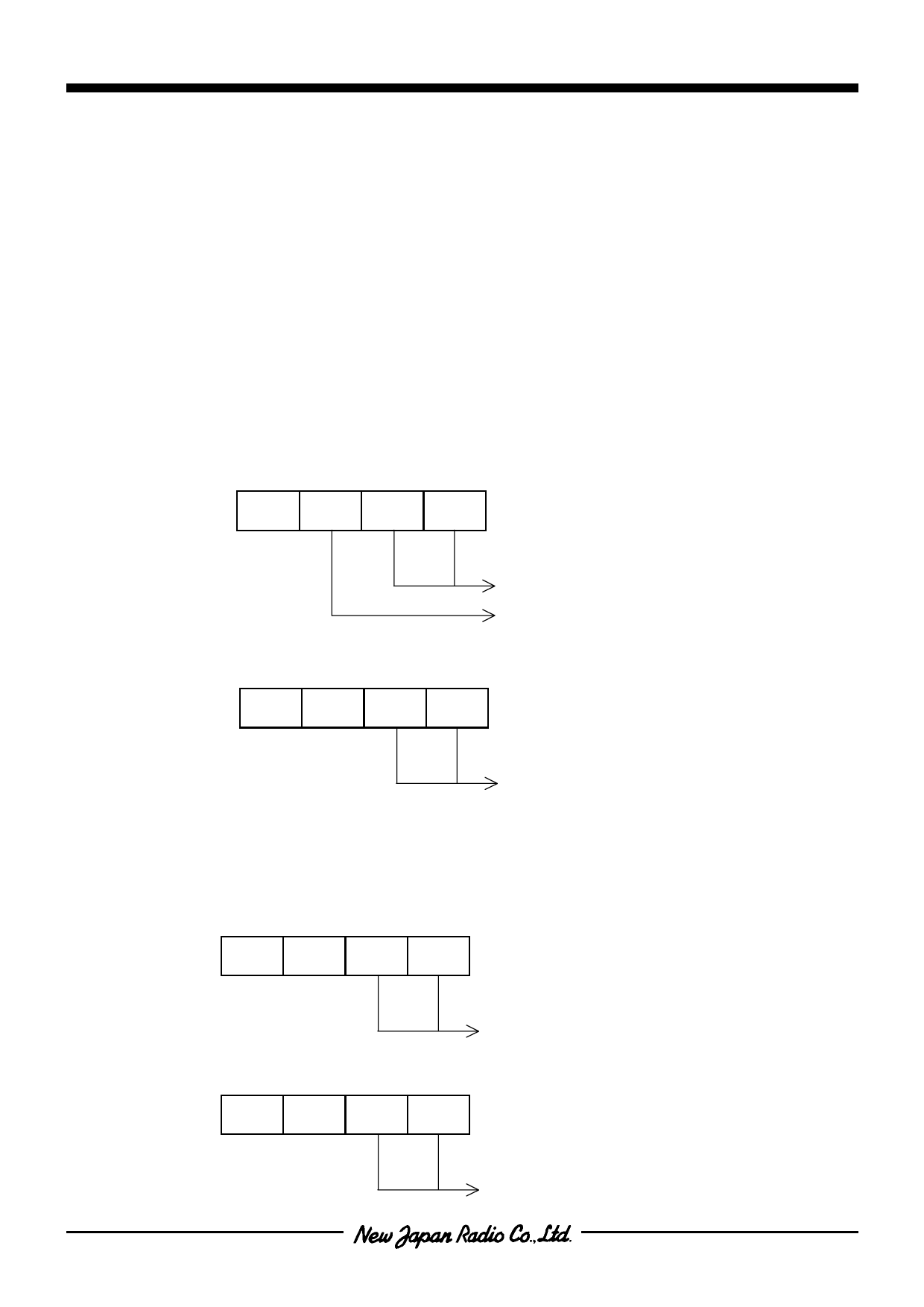
[READING PORTD INPUT DATA (PHY4)]
(MSB) 3
2
1
0 (LSB)
PHY4
“0” PD1E PD1 PD0
PORTD Input Data
1 : PD1 edge detection
[WRITING PORTD OUTPUT DATA (PHY4)]
(MSB) 3
2
1
0
(LSB)
PHY4
–
–
PD1 PD0
PORTD Output Data
• PORTE(PE0, PE1)
PORTE is a 2-bit input-output PORT. When the PORT is set as the output, the signal is output through
the output terminal by writing data to the PORTE register(PHY5). When the PORT is set as the input,
the external signal is gotten directly through the input terminal by reading data from PHY5.
[READING PORTE INPUT DATA (PHY5)]
(MSB) 3
2
1
0
PHY5
“0”
“0”
PE1 PE0
(LSB)
[WRITING PORTE OUTPUT DATA (PHY5)]
(MSB) 3
2
1
0
PHY5
–
–
PE1 PE0
PORTE Input Data
(LSB)
PORTE Output Data
- 10 -
Share Link: 