7641 데이터 시트보기 (PDF) - Mitsumi
부품명
상세내역
일치하는 목록
7641 Datasheet PDF : 149 Pages
| |||
PRELIMINARY NSocothimcaene:gpTeah.riasmisetnrioct laimfiintsalasrepescuibfijceacttioton.
MITSUBISHI MICROCOMPUTERS
7641 Group
SINGLE-CHIP 8-BIT CMOS MICROCOMPUTER
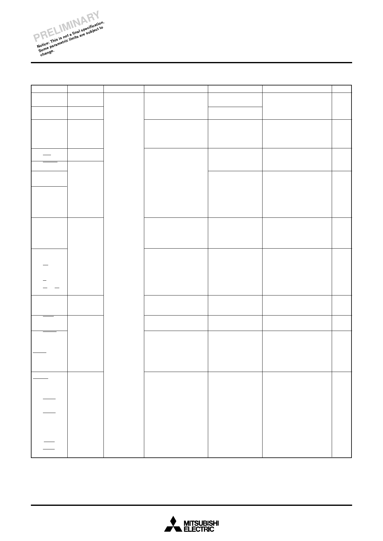
Table 6 List of I/O port function
Pin
P00/AB0–
P07/AB7
P10/AB8–
P17/AB15
P20/DB0–
P27/DB7
Name
Port P0
Port P1
Port P2
Input/Output
Input/Output,
individual bits
I/O format
CMOS input level
CMOS 3-state output
CMOS input level/VIHL
input level
CMOS 3-state output
P30/RDY–
P37/RD
P40/EDMA,
P41/INT0,
P42/INT1,
P43/CNTR0,
P44/CNTR1
Port P3
Port P4
CMOS input level
CMOS 3-state output
P50/XCIN,
P51/TOUT/
XCOUT
Port P5
P52/OBF0,
P53/IBF0,
P54/S0,
P55/A0,
P56/R(E),
P57/W(R/W)
P60/DQ0–
P67/DQ7
Port P6
P70/SOF,
Port P7
P71/HOLD,
P72/S1,
P73/IBF1/
HLDA,
P74/OBF1
P80/UTXD2/
SRDY,
P81/URXD2/
SCLK,
P82/CTS2/
SRXD,
P83/RTS2/
STXD,
P84/UTXD1,
P85/URXD1,
P86/CTS1,
P87/RTS1
Port P8
CMOS input level
CMOS 3-state output
CMOS input level
CMOS 3-state output
CMOS input level/TTL
input level in Master
CPU bus inferface
function
CMOS input level/TTL
input level
CMOS 3-state output
CMOS input level
CMOS 3-state output
CMOS input level
CMOS 3-state output
CMOS input level/TTL
input level in Master
CPU bus inferface
function
CMOS input level
CMOS 3-state output
Non-port function
Lower address
output
Higher address
output
Data bus I/O
Control signal I/O
Control signal I/O
External interrupt
Timer 1, Timer 2
output pin
Sub-clock generat-
ing input pin
Master CPU bus
interface I/O pin
Related SFRs
CPU mode register A
Port control register
Ref. No.
(1)
CPU mode register A
(2)
Port control register
Port P2 pull-up control
register
CPU mode register A
(1)
CPU mode register B
Port control register
(3)
CPU mode register A
(4)
CPU mode register B
(5)
Port control register
Timer X mode register
Timer Y mode register
Interrupt polarity select register
CPU mode register A
(6)
Port control register
(7)
Clock control register
Timer 123 mode register
Data bus buffer control
(8)
register 0
(9)
Port control register
(10)
Master CPU bus
Data bus buffer control
(11)
interface I/O pin
register 0
Port control register
USB function output USB control register
(12)
pin
Port control register
Control signal I/O
Data bus buffer control
(13)
Master CPU bus
register 1
(14)
interface I/O pin
Port control register
(15)
CPU mode register B
(16)
Serial I/O I/O pin
UART2 I/O pin
UART1 I/O pin
UART1, 2 control registers (17)
Serial I/O control register 1 (18)
Serial I/O control register 2 (19)
Port control register
(20)
(21)
(22)
(23)
(24)
Notes 1: For details of the ports functions in modes other than single-chip mode, and how to use double-function ports as function I/O ports, refer to the applicable
sections.
2: Make sure that the input level at each pin is either 0 V or VCC during execution of the STP instruction.
When an input level is at an intermediate potential, a rush current will flow from VCC to VSS through the input-stage gate.
15
Share Link: 