ADSP-21MSP58BST-104 데이터 시트보기 (PDF) - Analog Devices
부품명
상세내역
일치하는 목록
ADSP-21MSP58BST-104 Datasheet PDF : 40 Pages
| |||
ADSP-21msp58/59
DIGITAL ARCHITECTURE OVERVIEW
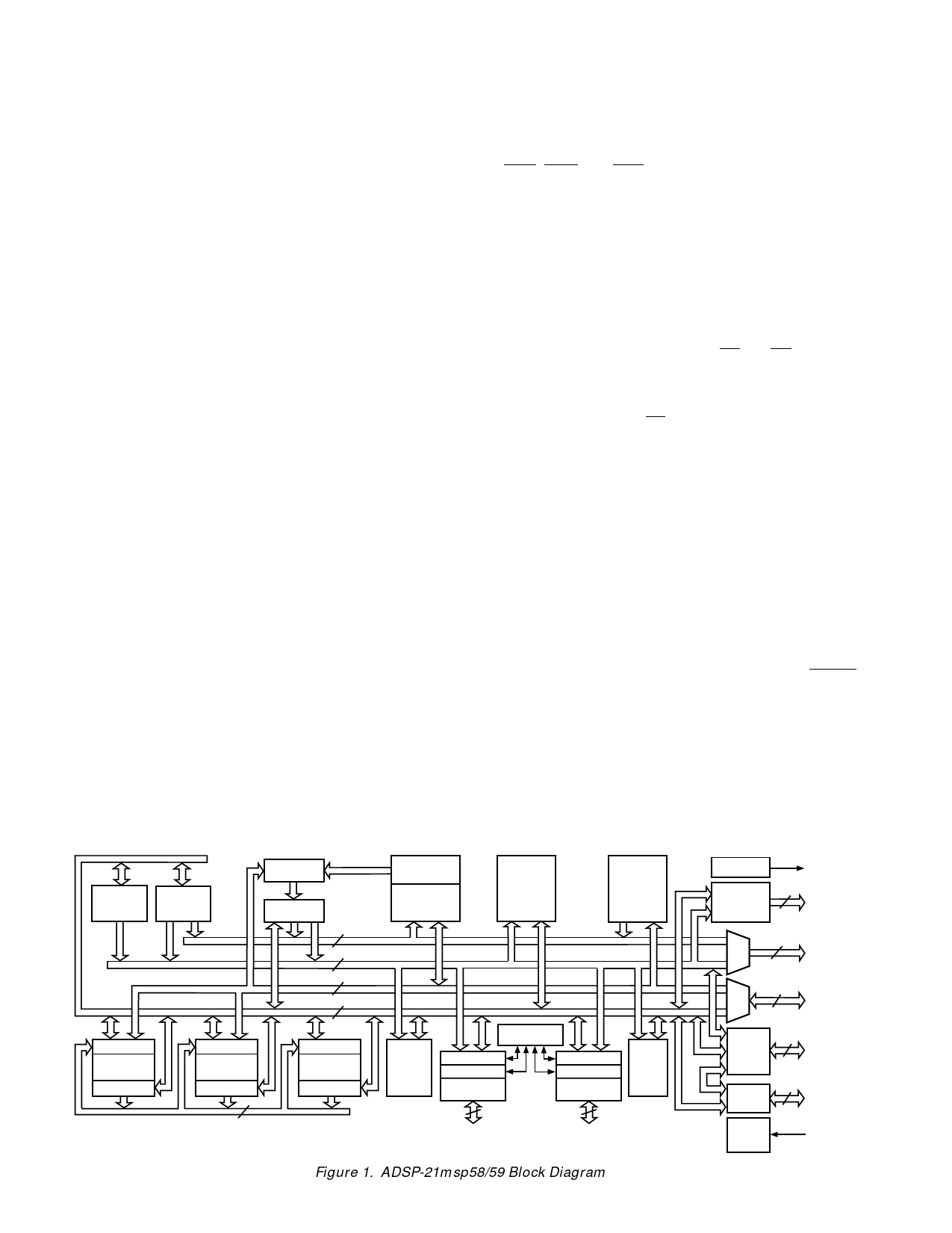
Figure 1 is an overall block diagram of the ADSP-21msp58/59.
The processors contain three independent computational units:
the ALU, the multiplier/accumulator (MAC), and the shifter.
The computational units process 16-bit data directly and have
provisions to support multiprecision computations. The ALU
performs a standard set of arithmetic and logic operations; divi-
sion primitives are also supported. The MAC performs single-
cycle multiply, multiply/add, and multiply/subtract operations.
The shifter performs logical and arithmetic shifts, normalization,
denormalization, and derive exponent operations. The shifter
can be used to efficiently implement numeric format control in-
cluding multiword floating-point representations.
The internal result (R) bus directly connects the computational
units so that the output of any unit may be the input of any unit
on the next cycle.
A powerful program sequencer and two dedicated data address
generators ensure efficient use of these computational units.
The sequencer supports conditional jumps, subroutine calls,
and returns in a single cycle. With internal loop counters and
loop stacks, the ADSP-21msp58/59 executes looped code with
zero overhead—no explicit jump instructions are required to
maintain the loop.
Two data address generators (DAGs) provide addresses for si-
multaneous dual operand fetches (from data memory and pro-
gram memory). Each DAG maintains and updates four address
pointers. Whenever the pointer is used to access data (indirect
addressing), it is post-modified by the value of one of four
modify registers. A length value may be associated with each
pointer to implement automatic modulo addressing for circular
buffers. The circular buffering feature is also used by the serial
ports for automatic data transfers to (and from) on-chip
memory.
Efficient data transfer is achieved with the use of five internal
buses:
• Program Memory Address (PMA) Bus
• Program Memory Data (PMD) Bus
• Data Memory Address (DMA) Bus
• Data Memory Data (DMD) Bus
• Result (R) Bus
The two address buses (PMA, DMA) share a single external ad-
dress bus, allowing memory to be expanded off chip, and the
two data buses (PMD, DMD) share a single external data bus.
The BMS, DMS, and PMS signals indicate which memory
space the external buses are being used for.
Program memory can store both instructions and data, permit-
ting the ADSP-21msp58/59 to fetch two operands in a single
cycle, one from program memory and one from data memory.
The ADSP-21msp58/59 can fetch an operand from on-chip
program memory and the next instruction in the same cycle.
The memory interface supports slow memories and memory-
mapped peripherals with programmable wait state generation.
External devices can gain control of the processors’ buses with
the use of the bus request/grant signals (BR and BG). Bus grant
has two modes of operation. If GoMode is enabled in the MSTAT
register, instruction execution continues from internal memory.
If GoMode is disabled, the processor stops instruction execution
and waits for deassertion of BR.
In addition to the address and data bus for external memory
connection, the ADSP-21msp58/59 has a host interface port
(HIP) for easy connection to a host processor. The HIP is made
up of 8 data/address pins and 10 control pins. The HIP is ex-
tremely flexible and provides a simple interface to a variety of
host processors. For example, the Motorola 68000 series, the
Intel 80C51 series, and the Analog Devices ADSP-2101 can be
easily connected to the HIP. The host processor can boot the
ADSP-21msp58/59 on-chip memory through the HIP.
The ADSP-21msp58/59 can respond to eleven interrupts. There
can be up to three external interrupts, configured as edge- or
level-sensitive, and seven internal interrupts generated by the
Timer, the Serial Ports (SPORTs), the HIP, the powerdown cir-
cuitry, and the analog interface. There is also a master RESET
signal.
The two serial ports provide a complete synchronous serial in-
terface with optional companding in hardware and a wide vari-
ety of framed or frameless data transmit and receive modes of
operation. Each port can generate an internal programmable se-
rial clock or accept an external serial clock.
Booting circuitry provides for loading on-chip program memory
automatically from byte-wide external memory. After reset,
DATA
ADDRESS
GENERATOR
#1
DATA
ADDRESS
GENERATOR
#2
INSTRUCTION
REGISTER
PROGRAM
SEQUENCER
PROGRAM
SRAM
2K x 24
PROGRAM
ROM
4K x 24
(ADSP-21msp59)
14 PMA BUS
14 DMA BUS
24 PMD BUS
16 DMD BUS
DATA
SRAM
2K x 16
BOOT
ADDRESS
GENERATOR
INPUT REGS
ALU
OUTPUT REGS
INPUT REGS
MAC
OUTPUT REGS
INPUT REGS
SHIFTER
OUTPUT REGS
16 R BUS
CONTROL
LOGIC
COMPANDING
CIRCUITRY
TRANSMIT REG
RECEIVE REG
SERIAL
PORT 0
TRANSMIT REG
RECEIVE REG
SERIAL
PORT 1
5
5
TIMER
Figure 1. ADSP-21msp58/59 Block Diagram
1
FLAG
ADC, DAC
7
AND
FILTERS
14
MUX
24
MUX
EXTERNAL
ADDRESS
BUS
EXTERNAL
DATA
BUS
10
HIP
CONTROL
HIP
8
REGISTER
POWER
DOWN
CONTROL
1
LOGIC
HIP
DATA
BUS
–2–
REV. 0
Share Link: 