ADSP-21MSP58BST-104 데이터 시트보기 (PDF) - Analog Devices
부품명
상세내역
일치하는 목록
ADSP-21MSP58BST-104 Datasheet PDF : 40 Pages
| |||
ADSP-21msp58/59
A signed ROM Verification Form and a purchase order for pro-
duction units are required prior to any product being manufac-
tured. Prototype units may be applied toward the minimum
order quantity.
Upon completion of prototype manufacture, Analog Devices
will ship prototype units and a delivery schedule update for pro-
duction units. An invoice against your purchase order for the
NRE charges is issued at this time.
There is a charge for each ROM mask generated and a mini-
mum order quantity. Consult your sales representative for de-
tails. A separate order must be placed for parts of a specific
package type, temperature range, and speed grade.
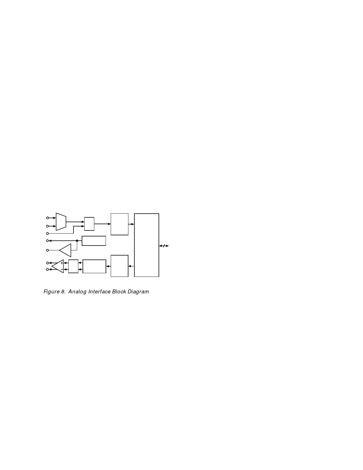
ANALOG INTERFACE
The analog interface contains encoding circuitry (ADC), decod-
ing circuitry (DAC), and processor interface logic. A block dia-
gram of the ADSP-21msp58/59 analog section is shown in
Figure 8.
The analog interface is configured through the Analog Control
Register and the Analog Autobuffer/Powerdown Register (refer
to “ADSP-21msp58/59 Registers”). The Analog Control Regis-
ter DM[0x3FEE] configures the programmable gain stages, the
analog input multiplexer, and the analog interface powerdown
state. Note that the unused bits must be cleared to zero.
VIN N ORM
VINAUX
DECOUPLE
REF_FILTER
VREF
MUX
BUF
ADC
PGA
VOLTAGE
REFERENCE
16-BIT
SIGMA-
DELTA
ADC
PROCESSOR 16
INTERFACE
VOUTP
VOUTN
DAC
PGA
OUTPUT
DIFFERENTIAL AMP
ANALOG
SMOOTHING
FILTER
16-BIT
SIGMA-
DELTA
DAC
Figure 8. Analog Interface Block Diagram
A/D Conversion
The A/D conversion circuitry of the analog interface consists of
an analog multiplexer, a programmable gain amplifier (ADC
PGA), and a 16-bit sigma-delta analog-to-digital converter
(ADC).
Analog Input Multiplexer and Amplifiers
The analog multiplexer selects either the NORM or AUX input
to the ADC’s sigma-delta modulator. The inputs should be ac
coupled.
The ADC PGA may be used to additionally increase the signal
level by +6 dB, +20 dB, or +26 dB. This gain is selected by bit
9 and bit 0 (IG0, IG1) of the analog control register. Input sig-
nal level to the sigma-delta ADC should not exceed the VINMAX
specification.
Analog-To-Digital Converter
The analog interface’s analog-to-digital converter consists of a
4th-order analog sigma-delta modulator, an anti-aliasing deci-
mation filter, and an optional digital high-pass filter. For a detailed
description of the ADC components, refer to the ADSP-2100
Family User’s Manual, Chapter 8, “Analog Interface.”
Bit 10 of the Analog Control Register (0x3FEE) may be set to
add an offset to the input of the ADC sigma-delta converter.
This offset moves ADC sigma-delta idle tones out of the 4.0
kHz speech band range. This added offset must be removed by
the ADC high-pass filter. Therefore, the high-pass filter must be
inserted when you use the offset feature.
D/A Conversion
The D/A conversion circuitry of the analog interface consists of
a sigma-delta digital-to-analog converter (DAC), an analog
smoothing filter, a programmable gain amplifier (DAC PGA),
and a differential output amplifier.
Digital-to-Analog Converter
The digital-to-analog converter consists of an optional digital
high-pass filter, an anti-imaging interpolation filter, and a
sigma-delta modulator. The digital filters and the sigma-delta
modulator have the same characteristics as the filters and
modulator of the ADC. For detailed description of the DAC
components, refer to the ADSP-2100 Family User’s Manual,
Chapter 8, “Analog Interface.”
Analog Smoothing Filter and Programmable Gain Amplifier
The analog smoothing filter consists of a 3rd-order switched ca-
pacitor filter with a 3 dB point at approximately 25 kHz.
The DAC’s programmable gain amplifier (DAC PGA) can be
used to adjust the output signal level by –15 dB to +6 dB in
3 dB increments. This gain is selected by bits 2–4 (OG0, OG1,
OG2) of the analog control register.
Differential Output Amplifier
The analog output signal (VOUTP, VOUTN) is produced by a
differential amplifier. The differential amplifier meets specifica-
tions for loads greater than 2 kΩ and has a maximum differen-
tial output swing of ± 3.156 V peak-to-peak (3.17 dBm0). The
DAC will drive loads smaller than 2 kΩ, but with degraded
performance.
The output signal is dc-biased to the on-chip voltage reference
(VREF) and can be ac-coupled directly to a load or dc-coupled to
an external amplifier.
The VOUTP, VOUTN output must be used as a differential sig-
nal otherwise performance will be severely compromised. Do
not use either pin as a single-ended output.
OPERATING THE ANALOG INTERFACE
The analog interface is operated with several memory-mapped
control and data registers. The ADC and DAC I/O data is re-
ceived and transmitted through two memory-mapped data regis-
ters. The data can also be autobuffered directly into (or from)
on-chip memory. In both cases, the I/O processing is interrupt
driven; two interrupts are dedicated to the analog interface, one
for the ADC receive data and one for the DAC transmit data.
The ADSP-21msp58/59 must have an input clock frequency of
13 MHz. At this frequency, analog-to-digital and digital-to-ana-
log converted data is transmitted at an 8 kHz rate with a single
16-bit word transmitted every 125 µs.
For detailed information about the analog interface, refer to the
ADSP-2100 Family User’s Manual, Chapter 8, “Analog Interface.”
–10–
REV. 0
Share Link: 