HEF4050BT 데이터 시트보기 (PDF) - NXP Semiconductors.
부품명
상세내역
일치하는 목록
HEF4050BT Datasheet PDF : 11 Pages
| |||
NXP Semiconductors
HEF4050B
Hex non-inverting buffers
Table 7. Dynamic characteristics …continued
VSS = 0 V; Tamb = 25 °C; for test circuit see Figure 6; unless otherwise specified.
Symbol Parameter
Conditions
VDD
Extrapolation formula
tTHL
HIGH to LOW
see Figure 5
5 V [1] 7 ns + (0.35 ns/pF)CL
output transition time
10 V
3 ns + (0.14 ns/pF)CL
15 V
2 ns + (0.09 ns/pF)CL
tTLH
LOW to HIGH
see Figure 5
5 V [1] 10 ns + (1.00 ns/pF)CL
output transition time
10 V
9 ns + (0.42 ns/pF)CL
15 V
6 ns + (0.28 ns/pF)CL
Min Typ Max Unit
-
25
50 ns
-
10
20 ns
-
7
14 ns
-
60 120 ns
-
30
60 ns
-
20
40 ns
[1] The typical values of the propagation delay and transition times are calculated from the extrapolation formulas shown (CL in pF).
Table 8. Dynamic power dissipation PD
PD can be calculated from the formulas shown. VSS = 0 V; tr = tf ≤ 20 ns; Tamb = 25 °C.
Symbol Parameter
VDD
Typical formula for PD (µW)
where:
PD
dynamic power 5 V
PD = 3800 × fi + Σ(fo × CL) × VDD2
fi = input frequency in MHz,
dissipation
10 V
PD = 11600 × fi + Σ(fo × CL) × VDD2
fo = output frequency in MHz,
15 V
PD = 65900 × fi + Σ(fo × CL) × VDD2
CL = output load capacitance in pF,
VDD = supply voltage in V,
Σ(CL × fo) = sum of the outputs.
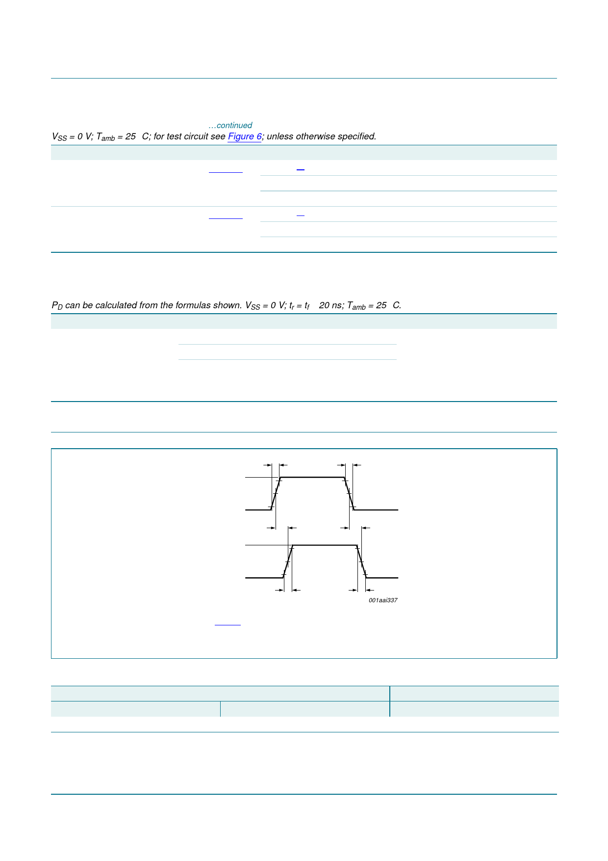
12. Waveforms
VI
input
10 %
0V
tr
90 %
VM
tPLH
VOH
output
VOL
VM
10 %
90 %
tTLH
tf
tPHL
tTHL
001aai337
Fig 5.
Measurement points are given in Table 9.
VOL and VOH are typical output voltage levels that occur with the output load.
Input to output propagation delays
Table 9.
Input
VM
0.5VDD
Measurement points
VI
0 V to VDD
Output
VM
0.5VDD
HEF4050B_5
Product data sheet
Rev. 05 — 11 November 2008
© NXP B.V. 2008. All rights reserved.
5 of 11
Share Link: 