HEF4050BT 데이터 시트보기 (PDF) - NXP Semiconductors.
부품명
상세내역
일치하는 목록
HEF4050BT Datasheet PDF : 11 Pages
| |||
NXP Semiconductors
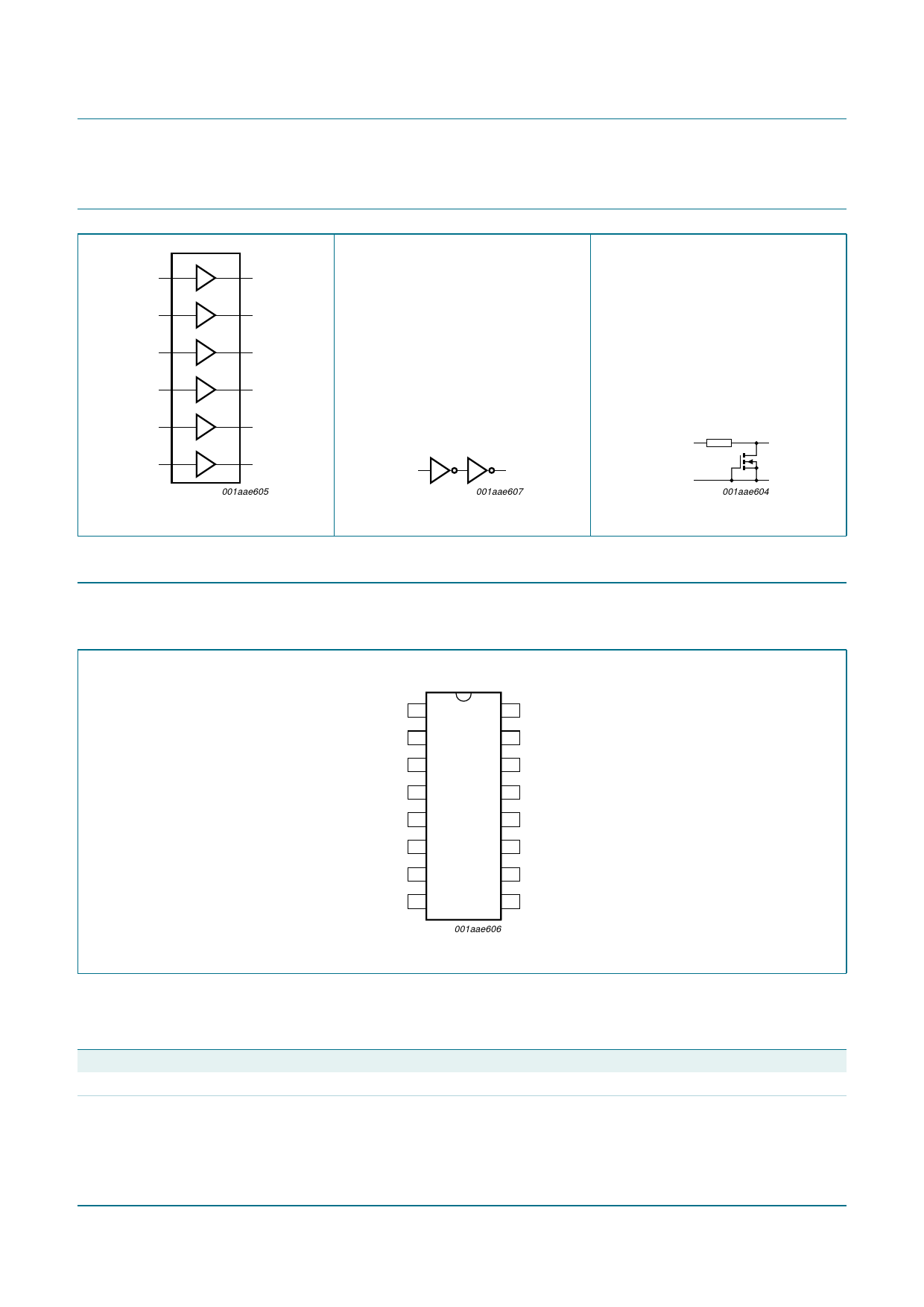
5. Functional diagram
HEF4050B
Hex non-inverting buffers
1A
3
1Y
2
2A
5
2Y
4
3A
7
3Y
6
9 4A
4Y 10
5A
11
5Y
12
14 6A
6Y 15
001aae605
Fig 1. Logic symbol
input
1A
1Y
001aae607
VSS
001aae604
Fig 2. Logic diagram for one gate Fig 3. Input protection circuit
6. Pinning information
6.1 Pinning
Fig 4. Pin configuration
HEF4050B
VDD 1
1Y 2
1A 3
2Y 4
2A 5
3Y 6
3A 7
VSS 8
16 n.c.
15 6Y
14 6A
13 n.c.
12 5Y
11 5A
10 4Y
9 4A
001aae606
6.2 Pin description
Table 2.
Symbol
VDD
1Y to 6Y
Pin description
Pin
1
2, 4, 6, 10, 12, 15
Description
supply voltage
output
HEF4050B_5
Product data sheet
Rev. 05 — 11 November 2008
© NXP B.V. 2008. All rights reserved.
2 of 11
Share Link: 